
Datasheet


74AHC_AHCT04 All information provided in this document is subject to legal disclaimers. © NXP B.V. 2011. All rights reserved.
Product data sheet Rev. 6 — 7 November 2011 3 of 15
NXP Semiconductors
74AHC04; 74AHCT04
hex inverter
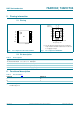
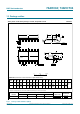
5. Pinning information
5.1 Pinning
5.2 Pin description
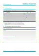
6. Functional description
[1] H = HIGH voltage level;
L = LOW voltage level.
(1) The die substrate is attached to the exposed die pad
using conductive die attach material. It can not be used
as a supply pin or input.
Fig 4. Pin configuration SO14 and TSSOP14 Fig 5. Pin configuration DHVQFN14
04
1A V
CC
1Y 6A
2A 6Y
2Y 5A
3A 5Y
3Y 4A
GND 4Y
001aac441
1
2
3
4
5
6
7
8
10
9
12
11
14
13
001aac442
04
GND
(1)
Transparent top view
3Y 4A
3A 5Y
2Y 5A
2A 6Y
1Y 6A
GND
4Y
1A
V
CC
6 9
5 10
4 11
3 12
2 13
7
8
1
14
terminal 1
index area
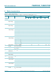
Table 2. Pin description
Symbol Pin Description
1A, 2A, 3A, 4A, 5A, 6A 1, 3, 5, 9, 11, 13 data input
1Y, 2Y, 3Y, 4Y, 5Y, 6Y 2, 4, 6, 8, 10, 12 data output
GND 7 ground (0 V)
V
CC
14 supply voltage
Table 3. Function table
[1]
Input nA Output nY
LH
HL