
Datasheet
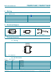

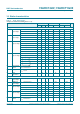
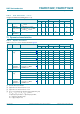
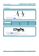
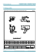
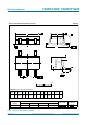
Table Of Contents
- 1. General description
- 2. Features and benefits
- 3. Ordering information
- 4. Marking
- 5. Functional diagram
- 6. Pinning information
- 7. Functional description
- 8. Limiting values
- 9. Recommended operating conditions
- 10. Static characteristics
- 11. Dynamic characteristics
- 12. Waveforms
- 13. Package outline
- 14. Abbreviations
- 15. Revision history
- 16. Legal information
- 17. Contact information
- 18. Contents
74AHC_AHCT1G02 All information provided in this document is subject to legal disclaimers. © NXP Semiconductors N.V. 2014. All rights reserved.
Product data sheet Rev. 7 — 6 November 2014 2 of 12
NXP Semiconductors
74AHC1G02; 74AHCT1G02
2-input NOR gate
4. Marking
[1] The pin 1 indicator is located on the lower left corner of the device, below the marking code.
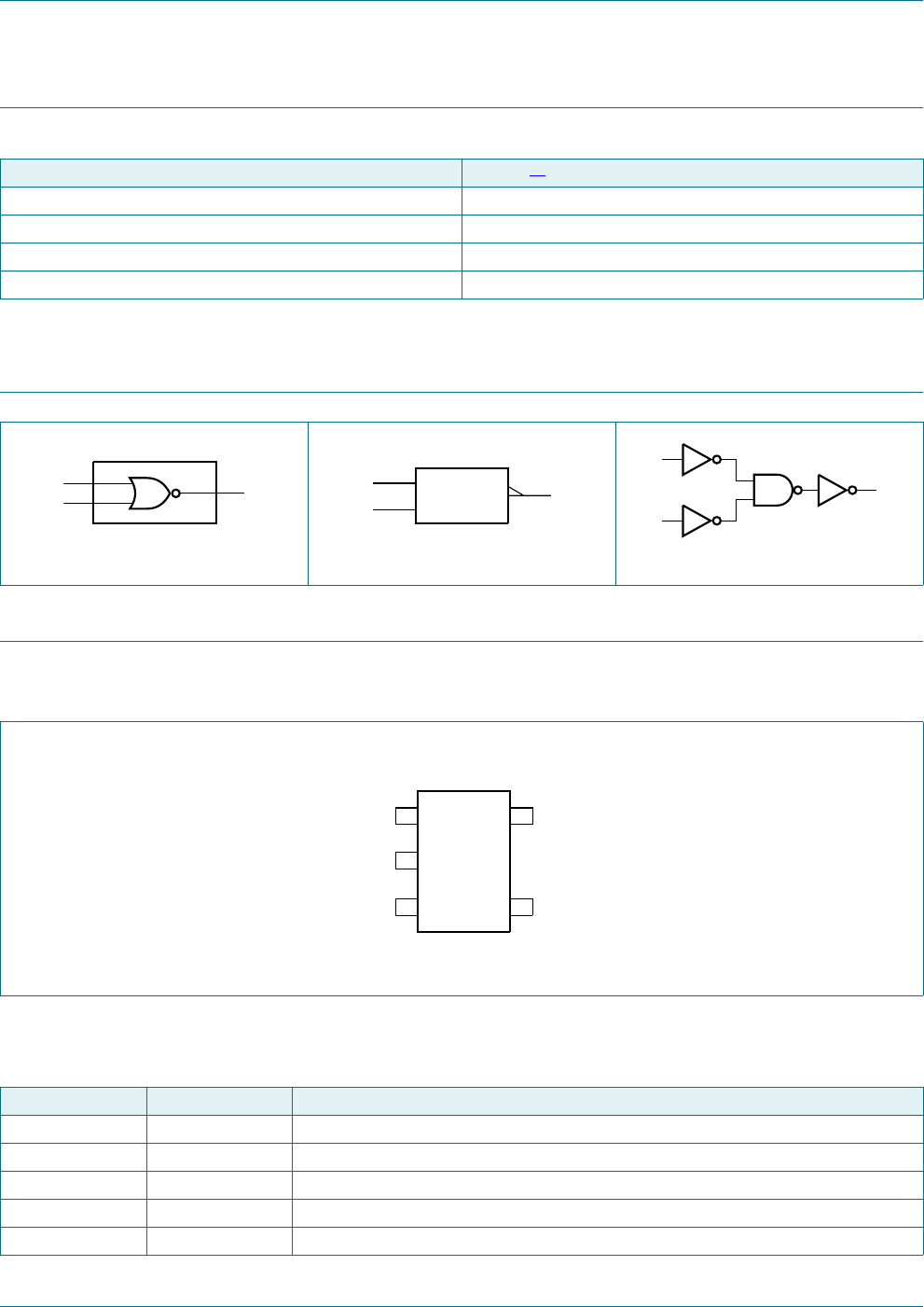
5. Functional diagram
6. Pinning information
6.1 Pinning
6.2 Pin description
Table 2. Marking codes
Type number Marking
[1]
74AHC1G02GW AB
74AHC1G02GV A02
74AHCT1G02GW CB
74AHCT1G02GV C02
Fig 1. Logic symbol Fig 2. IEC logic symbol Fig 3. Logic diagram
PQD
%
$
<
PQD
PQD
%
$
<
Fig 4. Pin configuration
$+&*
$+&7*
%9
&&
$
*1' <
DDI
Table 3. Pin description
Symbol Pin Description
B 1 data input B
A 2 data input A
GND 3 ground (0 V)
Y 4 data output Y
V
CC
5 supply voltage