
Datasheet


74AHC_AHCT1G08 All information provided in this document is subject to legal disclaimers. © NXP Semiconductors N.V. 2014. All rights reserved.
Product data sheet Rev. 7 — 18 November 2014 6 of 12
NXP Semiconductors
74AHC1G08; 74AHCT1G08
2-input AND gate
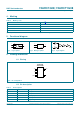
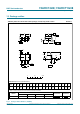
12. Waveforms
Measurement points are given in Tab le 9.
Fig 5. Input (A and B) to output (Y) propagation delays
PQD
$%LQSXW
<RXWSXW
W
3+/
W
3/+
9
0
9
0
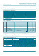
Table 9. Measurement point
Type Input Output
V
I
V
M
V
M
74AHC1G08 GND to V
CC
0.5 V
CC
0.5 V
CC
74AHCT1G08 GND to 3.0 V 1.5 V 0.5 V
CC
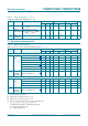
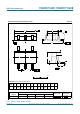
Test data is given in Table 8. Definitions for test circuit:
C
L
= Load capacitance including jig and probe capacitance.
R
T
= Termination resistance should be equal to output impedance Z
o
of the pulse generator.
Fig 6. Test circuit for measuring switching times
PQD
9
&&
9
,
9
2
5
7
&
/
38/6(
*(1(5$725
'87