
Datasheet

74AHC_AHCT02_4 © NXP B.V. 2008. All rights reserved.
Product data sheet Rev. 04 — 21 May 2008 3 of 14
NXP Semiconductors
74AHC02; 74AHCT02
Quad 2-input NOR gate
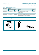
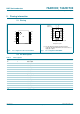
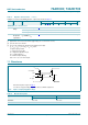
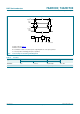
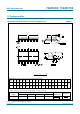
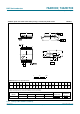
5. Pinning information
5.1 Pinning
5.2 Pin description
(1) The die substrate is attached to this pad using
conductive die attach material. It can not be used as a
supply pin or input.
Fig 4. Pin configuration SO14 and TSSOP14 Fig 5. Pin configuration DHVQFN14
02
1Y V
CC
1A 4Y
1B 4B
2Y 4A
2A 3Y
2B 3B
GND 3A
001aac919
1
2
3
4
5
6
7
8
10
9
12
11
14
13
001aac920
02
Transparent top view
2B 3B
2A 3Y
2Y 4A
1B 4B
1A 4Y
GND
3A
1Y
V
CC
6 9
5 10
4 11
3 12
2 13
7
8
1
14
terminal 1
index area
GND
(1)
Table 2. Pin description
Symbol Pin Description
1Y 1 data output
1A 2 data input
1B 3 data input
2Y 4 data output
2A 5 data input
2B 6 data input
GND 7 ground (0 V)
3A 8 data input
3B 9 data input
3Y 10 data output
4A 11 data input
4B 12 data input
4Y 13 data output
V
CC
14 supply voltage