
Datasheet


74AHC_AHCT14_5 © NXP B.V. 2009. All rights reserved.
Product data sheet Rev. 05 — 4 May 2009 7 of 16
NXP Semiconductors
74AHC14; 74AHCT14
Hex inverting Schmitt trigger
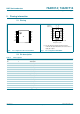
11. Waveforms
Measurement points are given in Table 8.
V
OL
and V
OH
are typical voltage output levels that occur with the output load.
Fig 6. Input to output propagation delays
mna344
t
PHL
t
PLH
V
M
V
M
V
M
V
M
nA input
nY output
GND
V
I
V
OH
V
OL
Table 8. Measurement points
Type Input Output
V
M
V
M
74AHC14 0.5 × V
CC
0.5 × V
CC
74AHCT14 1.5 V 0.5 × V
CC
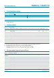
Test data is given in Table 9.
Definitions test circuit:
R
T
= Termination resistance should be equal to output impedance Z
o
of the pulse generator
C
L
= Load capacitance including jig and probe capacitance
Fig 7. Load circuitry for measuring switching times
001aah768
t
W
t
W
t
r
t
r
t
f
V
M
V
I
negative
pulse
GND
V
I
positive
pulse
GND
10 %
90 %
90 %
10 %
V
M
V
M
V
M
t
f
V
CC
DUT
R
T
V
I
V
O
C
L
G