
Datasheet


74AHC_AHCT164_3 © NXP B.V. 2008. All rights reserved.
Product data sheet Rev. 03 — 24 April 2008 10 of 18
NXP Semiconductors
74AHC164; 74AHCT164
8-bit serial-in/parallel-out shift register
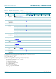
11. Waveforms
Measurement points are given in Table 8.
V
OL
and V
OH
are typical voltage output levels that occur with the output load.
Fig 7. Clock pulse width, maximum frequency and input to output propagation delays
001aac426
CP input
Qn
output
t
PHL
t
PLH
t
W
V
OH
V
I
GND
V
OL
V
M
V
M
1/f
max
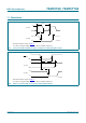
Measurement points are given in Table 8.
V
OL
and V
OH
are typical voltage output levels that occur with the output load.
Fig 8. Master reset pulse width, recovery time and propagation delays
001aac446
MR input
CP input
Qn output
t
PHL
t
WL
t
rec
V
M
V
I
GND
V
I
V
OH
V
OL
GND
V
M
V
M