
Datasheet


74AHC_AHCT1G79 All information provided in this document is subject to legal disclaimers. © NXP Semiconductors N.V. 2014. All rights reserved.
Product data sheet Rev. 6 — 23 September 2014 7 of 13
NXP Semiconductors
74AHC1G79; 74AHCT1G79
Single D-type flip-flop; positive-edge trigger
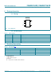
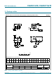
12. Waveforms
Measurement points are given in Table 9.
V
OL
and V
OH
are typical output voltage levels that occur with the output.
Fig 5. Clock (CP) to output (Q) propagation delay times, clock pulse width, D to set-up times, the CP to D hold
times and maximum clock pulse frequency
PQD
W
K
W
VX
W
K
W
3+/
W
:
W
3/+
W
VX
I
PD[
9
0
9
0
9
0
9
,
*1'
9
,
*1'
&3LQSXW
'LQSXW
9
2+
9
2/
4RXWSXW
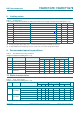
Table 9. Measurement points
Type Inputs Output
V
I
V
M
V
M
74AHC1G79 GND to V
CC
0.5 V
CC
0.5 V
CC
74AHCT1G79 GND to 3.0 V 1.5 V 0.5 V
CC
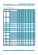
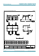
Test data is given in Table 8. Definitions for test circuit:
C
L
= Load capacitance including jig and probe capacitance.
R
T
= Termination resistance should be equal to output impedance Z
o
of the pulse generator.
Fig 6. Test circuit for measuring switching times
PQD
9
&&
9
,
9
2
5
7
&
/
38/6(
*(1(5$725
'87