
Datasheet


74AHC_AHCT245_5 © NXP B.V. 2009. All rights reserved.
Product data sheet Rev. 05 — 28 April 2009 4 of 16
NXP Semiconductors
74AHC245; 74AHCT245
Octal bus transceiver; 3-state
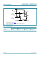
6. Functional description
[1] H = HIGH voltage level;
L = LOW voltage level;
X = don’t care;
Z = high-impedance OFF-state.
7. Limiting values
[1] The input and output voltage ratings may be exceeded if the input and output current ratings are observed.
[2] For SO20 packages: above 70 °C the value of P
tot
derates linearly at 8 mW/K.
For TSSOP20 packages: above 60 °C the value of P
tot
derates linearly at 5.5 mW/K.
For DHVQFN20 packages: above 60 °C the value of P
tot
derates linearly at 4.5 mW/K.
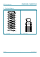
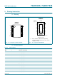
B1 17 data input/output
B0 18 data input/output
OE 19 output enable input (active LOW)
V
CC
20 supply voltage
Table 2. Pin description
…continued
Symbol Pin Description
Table 3. Function table
[1]
Control Input/output
OE DIR An Bn
L L A = B inputs
L H inputs B = A
HXZ Z
Table 4. Limiting values
In accordance with the Absolute Maximum Rating System (IEC 60134). Voltages are referenced to GND (ground = 0 V).
Symbol Parameter Conditions Min Max Unit
V
CC
supply voltage −0.5 +7.0 V
V
I
input voltage −0.5 +7.0 V
I
IK
input clamping current V
I
< −0.5 V
[1]
−20 - mA
I
OK
output clamping current V
O
< −0.5 V or V
O
>V
CC
+ 0.5 V
[1]
−20 +20 mA
I
O
output current V
O
= −0.5 V to (V
CC
+ 0.5 V) −25 +25 mA
I
CC
supply current - +75 mA
I
GND
ground current −75 - mA
T
stg
storage temperature −65 +150 °C
P
tot
total power dissipation T
amb
= −40 °C to +125 °C
[2]
- 500 mW