
Datasheet


74AHC_AHCT245_5 © NXP B.V. 2009. All rights reserved.
Product data sheet Rev. 05 — 28 April 2009 8 of 16
NXP Semiconductors
74AHC245; 74AHCT245
Octal bus transceiver; 3-state
[1] Typical values are measured at nominal supply voltage (V
CC
= 3.3 V and V
CC
= 5.0 V).
[2] t
pd
is the same as t
PLH
and t
PHL
.
[3] t
en
is the same as t
PZL
and t
PZH
.
[4] t
dis
is the same as t
PLZ
and t
PHZ
.
[5] C
PD
is used to determine the dynamic power dissipation (P
D
in µW).
P
D
=C
PD
× V
CC
2
× f
i
× N+Σ(C
L
× V
CC
2
× f
o
) where:
f
i
= input frequency in MHz;
f
o
= output frequency in MHz;
C
L
= output load capacitance in pF;
V
CC
= supply voltage in V;
N = number of inputs switching;
Σ(C
L
× V
CC
2
× f
o
) = sum of the outputs.
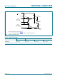
10.1 Waveforms
t
dis
disable time OE to An; OE to Bn;
signal name DIR;
see
Figure 6
[4]
C
L
= 15 pF - 5.0 14.4 1.0 15.5 1.0 18.0 ns
C
L
= 50 pF - 6.0 15.4 1.0 16.5 1.0 19.5 ns
C
PD
power
dissipation
capacitance
f
i
= 1 MHz;
V
I
= GND to V
CC
[5]
-15- - - - -pF
Table 7. Dynamic characteristics
…continued
Voltages are referenced to GND (ground = 0 V); for test circuit see Figure 7.
Symbol Parameter Conditions 25 °C −40 °C to +85 °C −40 °C to +125 °C Unit
Min Typ
[1]
Max Min Max Min Max
Measurement points are given in Table 8.
V
OL
and V
OH
are typical voltage output levels that occur with the output load.
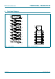
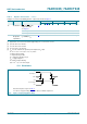
Fig 5. Input to output propagation delays
mna176
An,
Bn input
Bn,
An output
t
PLH
t
PHL
GND
V
I
V
M
V
M
V
M
V
M
V
OH
V
OL