
Datasheet


74AHC_AHCT273_3 © NXP B.V. 2008. All rights reserved.
Product data sheet Rev. 03 — 13 May 2008 4 of 18
NXP Semiconductors
74AHC273; 74AHCT273
Octal D-type flip-flop with reset; positive-edge trigger
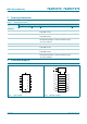
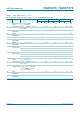
5. Pinning information
5.1 Pinning
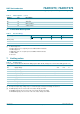
5.2 Pin description
(1) The die substrate is attached to this pad using
conductive die attach material. It can not be used as a
supply pin or input.
Fig 5. Pin configuration SO20 and TSSOP20 Fig 6. Pin configuration DHVQFN20
74AHC273
74AHCT273
MR V
CC
Q0 Q7
D0 D7
D1 D6
Q1 Q6
Q2 Q5
D2 D5
D3 D4
Q3 Q4
GND CP
001aai066
1
2
3
4
5
6
7
8
9
10
12
11
14
13
16
15
18
17
20
19
001aai067
74AHC273
74AHCT273
Transparent top view
Q4
D3
Q3
D4
D2 D5
Q2 Q5
Q1 Q6
D1 D6
D0 D7
Q0 Q7
GND
CP
MR
V
CC
9
12
8 13
7 14
6 15
5 16
4 17
3 18
2 19
10
11
1
20
terminal 1
index area
GND
(1)
Table 2. Pin description
Symbol Pin Description
MR 1 master reset input (active LOW)
Q0 2 flip-flop output
D0 3 data input
D1 4 data input
Q1 5 flip-flop output
Q2 6 flip-flop output
D2 7 data input
D3 8 data input
Q3 9 flip-flop output
GND 10 ground (0 V)
CP 11 clock input (LOW-to-HIGH edge-triggered)
Q4 12 flip-flop output
D4 13 data input
D5 14 data input
Q5 15 flip-flop output
Q6 16 flip-flop output