
Datasheet


74AHC_AHCT273_3 © NXP B.V. 2008. All rights reserved.
Product data sheet Rev. 03 — 13 May 2008 9 of 18
NXP Semiconductors
74AHC273; 74AHCT273
Octal D-type flip-flop with reset; positive-edge trigger
[1] Typical values are measured at nominal supply voltage (V
CC
= 3.3 V and V
CC
= 5.0 V).
[2] t
pd
is the same as t
PLH
and t
PHL
.
[3] t
pd
is the same as t
PHL
only.
[4] C
PD
is used to determine the dynamic power dissipation (P
D
in µW).
P
D
=C
PD
× V
CC
2
× f
i
× N+Σ(C
L
× V
CC
2
× f
o
) where:
f
i
= input frequency in MHz;
f
o
= output frequency in MHz;
C
L
= output load capacitance in pF;
V
CC
= supply voltage in V;
N = number of inputs switching;
Σ(C
L
× V
CC
2
× f
o
) = sum of the outputs.
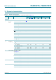
t
rec
recovery
time
MR to CP; see Figure 8
V
CC
= 3.0 V to 3.6 V 2.5 - - 2.5 - 2.5 - ns
V
CC
= 4.5 V to 5.5 V 2.0 - - 2.0 - 2.0 - ns
C
PD
power
dissipation
capacitance
f
i
= 1 MHz; V
I
= GND to V
CC
[4]
-14- - - - - pF
74AHCT273; V
CC
= 4.5 V to 5.5 V
t
pd
propagation
delay
CP to Qn; see Figure 7
[2]
C
L
= 15 pF - 4.0 7.5 1.0 8.8 1.0 9.5 ns
C
L
= 50 pF - 5.8 9.2 1.0 10.5 1.0 11.5 ns
MR to Qn; see Figure 8
[3]
C
L
= 15 pF - 3.9 10.0 1.0 11.6 1.0 12.5 ns
C
L
= 50 pF - 5.6 11.0 1.0 12.6 1.0 14.0 ns
f
max
maximum
frequency
see Figure 7
C
L
= 15 pF 75 120 - 65 - 65 - MHz
C
L
= 50 pF 50 75 - 45 - 45 - MHz
t
W
pulse width CP HIGH or LOW;
see
Figure 7
5.0 - - 6.5 - 6.5 - ns
MR LOW; see Figure 8 5.0 - - 6.0 - 6.0 - ns
t
su
set-up time Dn to CP; see Figure 9 3.0 - - 3.0 - 3.0 - ns
t
h
hold time Dn to CP; see Figure 9 1.0 - - 1.0 - 1.0 - ns
t
rec
recovery
time
MR to CP; see Figure 8 2.5 - - 2.5 - 2.5 - ns
C
PD
power
dissipation
capacitance
f
i
= 1 MHz; V
I
= GND to V
CC
[4]
-18- - - - - pF
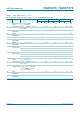
Table 7. Dynamic characteristics
…continued
Voltages are referenced to GND (ground = 0 V); for test circuit see Figure 10.
Symbol Parameter Conditions 25 °C −40 °C to +85 °C −40 °C to +125 °C Unit
Min Typ
[1]
Max Min Max Min Max