
Datasheet


74AHC_AHCT2G126 All information provided in this document is subject to legal disclaimers. © NXP B.V. 2013. All rights reserved.
Product data sheet Rev. 7 — 6 May 2013 7 of 16
NXP Semiconductors
74AHC2G126; 74AHCT2G126
Dual buffer/line driver; 3-state
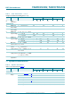
[1] t
pd
is the same as t
PLH
and t
PHL
.
t
en
is the same as t
PZL
and t
PZH
.
t
dis
is the same as t
PLZ
and t
PHZ
.
[2] Typical values are measured at V
CC
= 3.3 V.
[3] Typical values are measured at V
CC
= 5.0 V.
[4] C
PD
is used to determine the dynamic power dissipation P
D
(W).
P
D
=C
PD
V
CC
2
f
i
+ (C
L
V
CC
2
f
o
)where:
f
i
= input frequency in MHz;
f
o
= output frequency in MHz;
C
L
= output load capacitance in pF;
V
CC
= supply voltage in Volts.
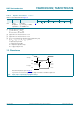
12. Waveforms
C
PD
power
dissipation
capacitance
per buffer;
C
L
=50pF;f
i
=1 MHz;
V
I
=GNDtoV
CC
[4]
-10- - - - - pF
Table 8. Dynamic characteristics
…continued
GND = 0 V; for test circuit see Figure 8.
Symbol Parameter Conditions 25 C 40 C to +85 C 40 C to +125 C Unit
Min Typ Max Min Max Min Max
Measurement points are given in Table 9.
Logic levels: V
OL
and V
OH
are typical output voltage levels that occur with the output load.
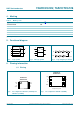
Fig 6. Input (nA) to output (nY) propagation delays
mna230
t
PHL
t
PLH
V
M
V
M
nA input
nY output
GND
V
I
V
OH
V
OL