
Datasheet


2003 Sep 08 2
Philips Semiconductors Product specification
Octal buffer/line driver; 3-state 74ALVC244
FEATURES
• Wide supply voltage range from 1.65 to 3.6 V
• 3.6 V tolerant inputs/outputs
• CMOS low power consumption
• Direct interface with TTL levels (2.7 to 3.6 V)
• Power-down mode
• Latch-up performance exceeds 250 mA
• Complies with JEDEC standard:
JESD8-7 (1.65 to 1.95 V)
JESD8-5 (2.3 to 2.7 V)
JESD8B/JESD36 (2.7 to 3.6 V)
• ESD protection:
HBM EIA/JESD22-A114-A exceeds 2000 V
MM EIA/JESD22-A115-A exceeds 200 V.
DESCRIPTION
The 74ALVC244 is a high-performance, low-power,
low-voltage, Si-gate CMOS device and superior to most
advanced CMOS compatible TTL families.
The 74ALVC244 is an octal non-inverting buffer/line driver
with 3-state outputs. The 3-state outputs are controlled by
the output enable inputs 1OE and 2OE. A HIGH on nOE
causes the outputs to assume a high-impedance
OFF-state. Schmitt-trigger action at all inputs makes the
circuit highly tolerant for slower input rise and fall times.
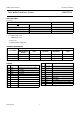
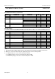
QUICK REFERENCE DATA
GND = 0 V; T
amb
=25°C.
Notes
1. C
PD
is used to determine the dynamic power dissipation (P
D
in µW).
P
D
=C
PD
× V
CC
2
× f
i
× N+Σ(C
L
× V
CC
2
× f
o
) where:
f
i
= input frequency in MHz;
f
o
= output frequency in MHz;
C
L
= output load capacitance in pF;
V
CC
= supply voltage in Volts;
N = total load switching outputs;
Σ(C
L
× V
CC
2
× f
o
) = sum of the outputs.
2. The condition is V
I
= GND to V
CC
.
SYMBOL PARAMETER CONDITIONS TYPICAL UNIT
t
PHL
/t
PLH
propagation delay nAn to nYn V
CC
= 1.8 V; C
L
= 30 pF; R
L
=1kΩ 2.7 ns
V
CC
= 2.5 V; C
L
= 30 pF; R
L
= 500 Ω 2.0 ns
V
CC
= 2.7 V; C
L
= 50 pF; R
L
= 500 Ω 2.3 ns
V
CC
= 3.3 V; C
L
= 50 pF; R
L
= 500 Ω 2.2 ns
C
I
input capacitance 3.5 pF
C
PD
power dissipation capacitance per buffer V
CC
= 3.3 V; notes 1 and 2 20 pF