
Datasheet


74ALVC245_2 © NXP B.V. 2008. All rights reserved.
Product data sheet Rev. 02 — 7 January 2008 3 of 14
NXP Semiconductors
74ALVC245
Octal bus transceiver; 3-state
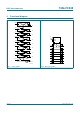
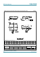
5. Pinning information
5.1 Pinning
5.2 Pin description
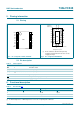
6. Functional description
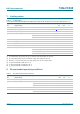
[1] H = HIGH voltage level; L = LOW voltage level; X = don’t care; Z = high-impedance OFF-state.
(1) The die substrate is attached to this pad using
conductive die attach material. It can not be used as
a supply pin or input.
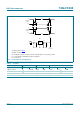
Fig 3. Pin configuration SO20, TSSOP20 Fig 4. Pin configuration DHVQFN20
245
DIR V
CC
A0 OE
A1 B0
A2 B1
A3 B2
A4 B3
A5 B4
A6 B5
A7 B6
GND B7
001aac431
1
2
3
4
5
6
7
8
9
10
12
11
14
13
16
15
18
17
20
19
001aac432
245
GND
(1)
Transparent top view
B6
A6
A7
B5
A5 B4
A4 B3
A3 B2
A2 B1
A1 B0
A0 OE
GND
B7
DIR
V
CC
9
12
8 13
7 14
6 15
5 16
4 17
3 18
2 19
10
11
1
20
terminal 1
index area
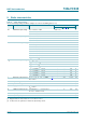
Table 2. Pin description
Symbol Pin Description
DIR 1 direction control
A[0:7] 2, 3, 4, 5, 6, 7, 8, 9 data input/output
B[0:7] 18, 17, 16, 15, 14, 13, 12,
11
data input/output
GND 10 ground (0 V)
OE 19 output enable input (active LOW)
V
CC
20 supply voltage
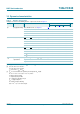
Table 3. Function table
[1]
Input Input/output
OE DIR An Bn
L L A = B input
L H input B = A
HXZZ