
Datasheet


74ALVC245_2 © NXP B.V. 2008. All rights reserved.
Product data sheet Rev. 02 — 7 January 2008 4 of 14
NXP Semiconductors
74ALVC245
Octal bus transceiver; 3-state
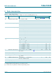
7. Limiting values
[1] The minimum input voltage ratings may be exceeded if the input current ratings are observed.
[2] The output voltage ratings may be exceeded if the output current ratings are observed.
[3] When V
CC
= 0 V (Power-down mode), the output voltage can be 3.6 V in normal operation.
[4] P
tot
derates linearly with 8 mW/K above 70 °C.
[5] P
tot
derates linearly with 5.5 mW/K above 60 °C.
[6] P
tot
derates linearly with 4.5 mW/K above 60 °C.
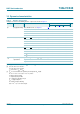
8. Recommended operating conditions
Table 4. Limiting values
In accordance with the Absolute Maximum Rating System (IEC 60134). Voltages are referenced to GND (ground = 0 V).
Symbol Parameter Conditions Min Max Unit
V
CC
supply voltage −0.5 +4.6 V
V
I
input voltage −0.5 +4.6 V
I
IK
input clamping current V
I
< 0 V
[1]
−50 - mA
I
OK
output clamping current V
O
>V
CC
or V
O
<0V - ±50 mA
V
O
output voltage output HIGH or LOW state
[2]
−0.5 V
CC
+ 0.5 V
output 3-state
[2]
−0.5 +4.6 V
power-down mode, V
CC
= 0 V
[3]
−0.5 +4.6 V
I
O
output current V
O
= 0 V to V
CC
- ±50 mA
I
CC
supply current - 100 mA
I
GND
ground current −100 - mA
T
stg
storage temperature −65 +150 °C
P
tot
total power dissipation T
amb
= −40 °C to +85 °C
SO20 package
[4]
- 500 mW
TSSOP20 package
[5]
- 500 mW
DHVQFN20 package
[6]
- 500 mW
Table 5. Recommended operating conditions
Symbol Parameter Conditions Min Max Unit
V
CC
supply voltage 1.65 3.6 V
V
I
input voltage 0 3.6 V
V
O
output voltage output HIGH or LOW state 0 V
CC
V
output 3-state 0 3.6 V
power-down mode, V
CC
= 0 V 0 3.6 V
T
amb
ambient temperature −40 +85 °C
∆t/∆V input transition rise and fall rate V
CC
= 1.65 V to 2.7 V - 20 ns/V
V
CC
= 2.7 V to 3.6 V - 10 ns/V