
Datasheet


1. General description
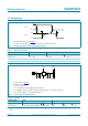
The 74AUP1G07 provides the single non-inverting buffer with open-drain output. The
output of the device is an open drain and can be connected to other open-drain outputs to
implement active-LOW wired-OR or active-HIGH wired-AND functions.
Schmitt-trigger action at all inputs makes the circuit tolerant to slower input rise and fall
times across the entire V
CC
range from 0.8 V to 3.6 V.
This device ensures a very low static and dynamic power consumption across the entire
V
CC
range from 0.8 V to 3.6 V.
This device is fully specified for partial power-down applications using I
OFF
.
The I
OFF
circuitry disables the output, preventing the damaging backflow current through
the device when it is powered down.
2. Features and benefits
Wide supply voltage range from 0.8 V to 3.6 V
High noise immunity
Complies with JEDEC standards:
JESD8-12 (0.8 V to 1.3 V)
JESD8-11 (0.9 V to 1.65 V)
JESD8-7 (1.2 V to 1.95 V)
JESD8-5 (1.8 V to 2.7 V)
JESD8-B (2.7 V to 3.6 V)
ESD protection:
HBM JESD22-A114F Class 3A exceeds 5000 V
MM JESD22-A115-A exceeds 200 V
CDM JESD22-C101E exceeds 1000 V
Low static power consumption; I
CC
= 0.9 A (maximum)
Latch-up performance exceeds 100 mA per JESD 78 Class II
Inputs accept voltages up to 3.6 V
Low noise overshoot and undershoot < 10 % of V
CC
I
OFF
circuitry provides partial Power-down mode operation
Multiple package options
Specified from 40 Cto+85C and 40 Cto+125C
74AUP1G07
Low-power buffer with open-drain output
Rev. 7 — 16 July 2012 Product data sheet