
Datasheet


74AUP1G07 All information provided in this document is subject to legal disclaimers. © NXP B.V. 2012. All rights reserved.
Product data sheet Rev. 7 — 16 July 2012 7 of 19
NXP Semiconductors
74AUP1G07
Low-power buffer with open-drain output
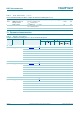
11. Dynamic characteristics
I
OFF
additional power-off
leakage current
V
I
or V
O
= 0 V to 3.6 V;
V
CC
=0Vto0.2 V
--0.75 A
I
CC
supply current V
I
= GND or V
CC
; I
O
= 0 A;
V
CC
= 0.8 V to 3.6 V
--1.4A
I
CC
additional supply current V
I
= V
CC
0.6 V; I
O
= 0 A; V
CC
=3.3V - - 75 A
Table 7. Static characteristics
…continued
At recommended operating conditions; voltages are referenced to GND (ground = 0 V).
Symbol Parameter Conditions Min Typ Max Unit
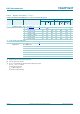
Table 8. Dynamic characteristics
Voltages are referenced to GND (ground = 0 V); for test circuit see Figure 9
.
Symbol Parameter Conditions 25 C 40 C to +125 C Unit
Min Typ
[1]
Max Min Max
(85 C)
Max
(125 C)
C
L
= 5 pF
t
pd
propagation delay A to Y; see Figure 8
[2]
V
CC
= 0.8 V - 11.6 - - - - ns
V
CC
= 1.1 V to 1.3 V 2.1 4.1 7.5 1.7 9.1 10.0 ns
V
CC
= 1.4 V to 1.6 V 1.6 3.0 5.1 1.3 6.1 6.7 ns
V
CC
= 1.65 V to 1.95 V 1.6 2.7 4.0 1.2 5.0 5.5 ns
V
CC
= 2.3 V to 2.7 V 1.1 2.1 3.2 0.9 4.0 4.4 ns
V
CC
= 3.0 V to 3.6 V 1.4 2.2 2.8 1.1 3.3 3.6 ns
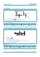
C
L
= 10 pF
t
pd
propagation delay A to Y; see Figure 8
[2]
V
CC
= 0.8 V - 14.7 - - - - ns
V
CC
= 1.1 V to 1.3 V 3.0 5.1 9.0 2.4 11.2 12.3 ns
V
CC
= 1.4 V to 1.6 V 2.3 3.8 6.1 2.0 7.4 8.1 ns
V
CC
= 1.65 V to 1.95 V 2.4 3.6 4.8 1.8 6.1 6.7 ns
V
CC
= 2.3 V to 2.7 V 1.7 2.8 3.8 1.3 4.8 5.3 ns
V
CC
= 3.0 V to 3.6 V 2.2 3.1 4.2 1.6 4.5 5.0 ns
C
L
= 15 pF
t
pd
propagation delay A to Y; see Figure 8
[2]
V
CC
= 0.8 V - 17.7 - - - - ns
V
CC
= 1.1 V to 1.3 V 3.5 6.1 10.4 3.2 13.1 14.5 ns
V
CC
= 1.4 V to 1.6 V 3.0 4.5 6.8 2.6 8.6 9.4 ns
V
CC
= 1.65 V to 1.95 V 2.8 4.4 6.7 2.2 7.8 8.6 ns
V
CC
= 2.3 V to 2.7 V 2.4 3.4 4.5 1.9 5.3 5.8 ns
V
CC
= 3.0 V to 3.6 V 2.2 4.0 5.7 1.9 6.1 6.7 ns