
Datasheet


74AUP1G07 All information provided in this document is subject to legal disclaimers. © NXP B.V. 2012. All rights reserved.
Product data sheet Rev. 7 — 16 July 2012 9 of 19
NXP Semiconductors
74AUP1G07
Low-power buffer with open-drain output
12. Waveforms
[1] For measuring enable and disable times, R
L
= 5 k, for measuring propagation delays, setup and hold times and pulse width, R
L
= 1
M.
Measurement points are given in Table 9
.
Logic level: V
OL
is the typical output voltage level that occurs with the output load.
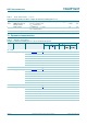
Fig 8. The data input (A) to output (Y) propagation delays
mna626
t
PLZ
V
X
Y output
A input
V
I
V
CC
V
M
V
OL
GND
t
PZL
V
M
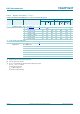
Table 9. Measurement points
Supply voltage Input Output
V
CC
V
M
V
M
V
X
0.8 V to 1.6 V 0.5 V
CC
0.5 V
CC
V
OL
+0.1V
1.65 V to 2.7 V 0.5 V
CC
0.5 V
CC
V
OL
+0.15V
3.0 V to 3.6 V 0.5 V
CC
0.5 V
CC
V
OL
+0.3V
Test data is given in Table 10.
Definitions for test circuit:
R
L
= Load resistance.
C
L
= Load capacitance including jig and probe capacitance.
R
T
= Termination resistance should be equal to the output impedance Z
o
of the pulse generator.
V
EXT
= External voltage for measuring switching times.
Fig 9. Load circuitry for switching times
001aac521
DUT
R
T
V
I
V
O
V
EXT
V
CC
R
L
5 kΩ
C
L
G
Table 10. Test data
Supply voltage Load V
EXT
V
CC
C
L
R
L
[1]
t
PLH
, t
PHL
t
PZH
, t
PHZ
t
PZL
, t
PLZ
0.8 V to 3.6 V 5 pF, 10 pF, 15 pF and 30 pF 5 k or 1 M open GND 2 V
CC