
Datasheet


74AUP1G0832 All information provided in this document is subject to legal disclaimers. © NXP B.V. 2012. All rights reserved.
Product data sheet Rev. 5 — 22 June 2012 10 of 19
NXP Semiconductors
74AUP1G0832
Low-power 3-input AND-OR gate
[1] For measuring enable and disable times R
L
= 5 kΩ, for measuring propagation delays, setup and hold times and pulse width R
L
= 1 MΩ.
Table 10. Measurement points
Supply voltage Output Input
V
CC
V
M
V
M
V
I
t
r
= t
f
0.8 V to 3.6 V 0.5 × V
CC
0.5 × V
CC
V
CC
≤ 3.0 ns
Test data is given in Table 11.
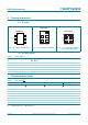
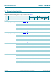
Definitions for test circuit:
R
L
= Load resistance.
C
L
= Load capacitance including jig and probe capacitance.
R
T
= Termination resistance should be equal to the output impedance Z
o
of the pulse generator.
V
EXT
= External voltage for measuring switching times.
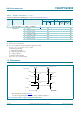
Fig 10. Load circuitry for switching times
001aac521
DUT
R
T
V
I
V
O
V
EXT
V
CC
R
L
5 kΩ
C
L
G
Table 11. Test data
Supply voltage Load V
EXT
V
CC
C
L
R
L
[1]
t
PLH
, t
PHL
t
PZH
, t
PHZ
t
PZL
, t
PLZ
0.8 V to 3.6 V 5 pF, 10 pF, 15 pF and 30 pF 5 kΩ or 1 MΩ open GND 2 × V
CC