
Datasheet


74AUP1G0832 All information provided in this document is subject to legal disclaimers. © NXP B.V. 2012. All rights reserved.
Product data sheet Rev. 5 — 22 June 2012 3 of 19
NXP Semiconductors
74AUP1G0832
Low-power 3-input AND-OR gate
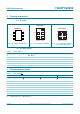
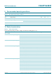
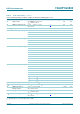
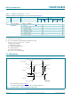
6. Pinning information
6.1 Pinning
6.2 Pin description
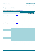
7. Functional description
[1] H = HIGH voltage level; L = LOW voltage level.
Fig 2. Pin configuration SOT363 Fig 3. Pin configuration SOT886 Fig 4. Pin configuration SOT891,
SOT1115 and SOT1202
74AUP1G0832
AC
GND
BY
001aad940
1
2
3
6
V
CC
5
4
74AUP1G0832
GND
001aad941
A
B
V
CC
C
Y
Transparent top view
2
3
1
5
4
6
74AUP1G0832
GND
001aad942
A
B
V
CC
C
Y
Transparent top view
2
3
1
5
4
6
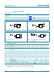
Table 3. Pin description
Symbol Pin Description
A 1 data input A
GND 2 ground (0 V)
B 3 data input B
Y 4 data output Y
V
CC
5 supply voltage
C 6 data input C
Table 4. Function table
[1]
Input Output
C B A Y
LLLL
LLHL
LHLL
LHHH
HL L H
HL HH
HHL H
HHHH