
Datasheet


74AUP1G0832 All information provided in this document is subject to legal disclaimers. © NXP B.V. 2012. All rights reserved.
Product data sheet Rev. 5 — 22 June 2012 4 of 19
NXP Semiconductors
74AUP1G0832
Low-power 3-input AND-OR gate
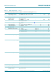
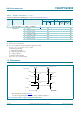
7.1 Logic configurations
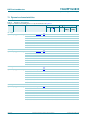
8. Limiting values
[1] The minimum input and output voltage ratings may be exceeded if the input and output current ratings are observed.
[2] For SC-88 packages: above 87.5 °C the value of P
tot
derates linearly with 4.0 mW/K.
For XSON6 packages: above 118 °C the value of P
tot
derates linearly with 7.8 mW/K.
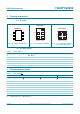
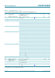
Table 5. Function selection table
Logic function Figure
2-input AND see Figure 5
2-input OR see Figure 6 and 7
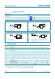
3-input gate with the Boolean function: Y = (A × B) + C see Figure 8
Fig 5. 2-input AND gate Fig 6. 2-input OR gate
001aad944
1
2
3
6
5
4Y
V
CC
B
A
A
B
Y
001aad945
1
2
3
6
5
4Y
Y
C
B
B
C
V
CC
Fig 7. 2-input OR gate Fig 8. 3-input gate with the Boolean function:
Y=(A× B) + C
001aad946
1
2
3
6
5
4Y
Y
C
A
A
C
V
CC
001aad947
1
2
3
6
5
4Y
C
A
B
V
CC
A
B
C
Y
Table 6. Limiting values
In accordance with the Absolute Maximum Rating System (IEC 60134). Voltages are referenced to GND (ground = 0 V).
Symbol Parameter Conditions Min Max Unit
V
CC
supply voltage −0.5 +4.6 V
I
IK
input clamping current V
I
<0V −50 - mA
V
I
input voltage
[1]
−0.5 +4.6 V
I
OK
output clamping current V
O
<0V −50 - mA
V
O
output voltage Active mode and Power-down mode
[1]
−0.5 +4.6 V
I
O
output current V
O
=0 VtoV
CC
- ±20 mA
I
CC
supply current - 50 mA
I
GND
ground current −50 - mA
T
stg
storage temperature −65 +150 °C
P
tot
total power dissipation T
amb
= −40 °C to +125 °C
[2]
- 250 mW