
Datasheet


74AUP1G08 All information provided in this document is subject to legal disclaimers. © NXP B.V. 2012. All rights reserved.
Product data sheet Rev. 6 — 22 June 2012 10 of 21
NXP Semiconductors
74AUP1G08
Low-power 2-input AND gate
[1] t
pd
is the same as t
PLH
and t
PHL
.
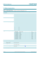
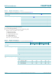
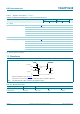
12. Waveforms
C
L
= 15 pF
t
pd
propagation delay A, B to Y; see Figure 8
[1]
V
CC
= 1.1 V to 1.3 V 3.1 15.7 3.1 17.3 ns
V
CC
= 1.4 V to 1.6 V 2.1 10.1 2.1 11.2 ns
V
CC
= 1.65 V to 1.95 V 1.8 8.2 1.8 9.0 ns
V
CC
= 2.3 V to 2.7 V 1.6 6.5 1.6 7.2 ns
V
CC
= 3.0 V to 3.6 V 1.5 5.9 1.5 6.5 ns
C
L
= 30 pF
t
pd
propagation delay A, B to Y; see Figure 8
[1]
V
CC
= 1.1 V to 1.3 V 4.1 21.8 4.1 24.0 ns
V
CC
= 1.4 V to 1.6 V 2.9 13.6 2.9 15.0 ns
V
CC
= 1.65 V to 1.95 V 2.4 10.9 2.4 12.1 ns
V
CC
= 2.3 V to 2.7 V 2.2 8.6 2.2 9.5 ns
V
CC
= 3.0 V to 3.6 V 2.1 7.5 2.1 8.3 ns
Table 9. Dynamic characteristics
…continued
Voltages are referenced to GND (ground = 0 V); for test circuit see Figure 9
Symbol Parameter Conditions −40 °C to +85 °C −40 °C to +125 °C Unit
Min Max Min Max
Measurement points are given in Table 10.
Logic levels: V
OL
and V
OH
are typical output voltage drops that occur with the output load.
Fig 8. The data input (A or B) to output (Y) propagation delays
mna614
t
PHL
t
PLH
V
M
V
M
A, B input
Y output
GND
V
I
V
OH
V
OL
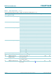
Table 10. Measurement points
Supply voltage Output Input
V
CC
V
M
V
M
V
I
t
r
= t
f
0.8 V to 3.6 V 0.5 × V
CC
0.5 × V
CC
V
CC
≤ 3.0 ns