
Datasheet


74AUP1G132 All information provided in this document is subject to legal disclaimers. © NXP B.V. 2012. All rights reserved.
Product data sheet Rev. 5 — 29 June 2012 2 of 22
NXP Semiconductors
74AUP1G132
Low-power 2-input NAND Schmitt trigger
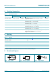
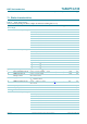
4. Ordering information
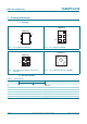
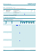
5. Marking
[1] The pin 1 indicator is located on the lower left corner of the device, below the marking code.
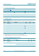
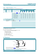
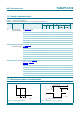
6. Functional diagram
Table 1. Ordering information
Type number Package
Temperature range Name Description Version
74AUP1G132GW 40 C to +125 C TSSOP5 plastic thin shrink small outline package; 5 leads;
body width 1.25 mm
SOT353-1
74AUP1G132GM 40 C to +125 C XSON6 plastic extremely thin small outline package; no leads;
6 terminals; body 1 1.45 0.5 mm
SOT886
74AUP1G132GF 40 C to +125 C XSON6 plastic extremely thin small outline package; no leads;
6 terminals; body 1 1 0.5 mm
SOT891
74AUP1G132GN 40 C to +125 C XSON6 extremely thin small outline package; no leads;
6 terminals; body 0.9 1.0 0.35 mm
SOT1115
74AUP1G132GS 40 C to +125 C XSON6 extremely thin small outline package; no leads;
6 terminals; body 1.0 1.0 0.35 mm
SOT1202
74AUP1G132GX 40 C to +125 C X2SON5 X2SON5: plastic thermal enhanced extremely thin
small outline package; no leads; 5 terminals;
body 0.8 0.8 0.35 mm
SOT1226
Table 2. Marking
Type number Marking code
[1]
74AUP1G132GW aE
74AUP1G132GM aE
74AUP1G132GF aE
74AUP1G132GN aE
74AUP1G132GS aE
74AUP1G132GX aE
Fig 1. Logic symbol Fig 2. IEC logic symbol Fig 3. Logic diagram
mna097
B
A
Y
2
1
4
mna098
2
4
&
1
001aac532
Y
B
A