
Datasheet


74AUP1G14 All information provided in this document is subject to legal disclaimers. © NXP B.V. 2012. All rights reserved.
Product data sheet Rev. 6 — 28 June 2012 13 of 24
NXP Semiconductors
74AUP1G14
Low-power Schmitt trigger inverter
16. Application information
The slow input rise and fall times cause additional power dissipation, this can be
calculated using the following formula:
P
ad
=f
i
× (t
r
× I
CC(AV)
+t
f
× I
CC(AV)
) × V
CC
where:
P
ad
= additional power dissipation (μW);
f
i
= input frequency (MHz);
t
r
= input rise time (ns); 10 % to 90 %;
t
f
= input fall time (ns); 90 % to 10 %;
I
CC(AV)
= average additional supply current (μA).
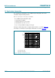
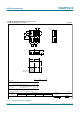
Average I
CC
differs with positive or negative input transitions, as shown in Figure 14.
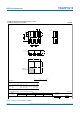
An example of a relaxation circuit using the 74AUP1G14 is shown in Figure 15
.
(1) Positive-going edge
(2) Negative-going edge.
Fig 14. Average I
CC
as a function of V
CC
001aad027
V
CC
(V)
0.8 3.82.81.8
0.1
0.2
0.3
ΔI
CC(AV)
(mA)
0
(1)
(2)