
Datasheet


74AUP1G14 All information provided in this document is subject to legal disclaimers. © NXP B.V. 2012. All rights reserved.
Product data sheet Rev. 6 — 28 June 2012 9 of 24
NXP Semiconductors
74AUP1G14
Low-power Schmitt trigger inverter
[1] For measuring enable and disable times R
L
= 5 kΩ, for measuring propagation delays, setup and hold times and pulse width R
L
= 1 MΩ.
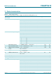
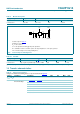
14. Transfer characteristics
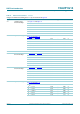
Table 9. Measurement points
Supply voltage Output Input
V
CC
V
M
V
M
V
I
t
r
= t
f
0.8 V to 3.6 V 0.5 × V
CC
0.5 × V
CC
V
CC
≤ 3.0 ns
Test data is given in Table 10.
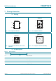
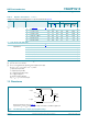
Definitions for test circuit:
R
L
= Load resistance.
C
L
= Load capacitance including jig and probe capacitance.
R
T
= Termination resistance should be equal to the output impedance Z
o
of the pulse generator.
V
EXT
= External voltage for measuring switching times.
Fig 9. Load circuitry for switching times
001aac521
DUT
R
T
V
I
V
O
V
EXT
V
CC
R
L
5 kΩ
C
L
G
Table 10. Test data
Supply voltage Load V
EXT
V
CC
C
L
R
L
[1]
t
PLH
, t
PHL
t
PZH
, t
PHZ
t
PZL
, t
PLZ
0.8 V to 3.6 V 5 pF, 10 pF, 15 pF and 30 pF 5 kΩ or 1 MΩ open GND 2 × V
CC
Table 11. Transfer characteristics
Voltages are referenced to GND (ground = 0 V); for test circuit see Figure 9
.
Symbol Parameter Conditions Min Typ Max Unit
T
amb
= 25 °C
V
T+
positive-going
threshold voltage
see Figure 10 and Figure 11
V
CC
= 0.8 V 0.30 - 0.60 V
V
CC
= 1.1 V 0.53 - 0.90 V
V
CC
= 1.4 V 0.74 - 1.11 V
V
CC
= 1.65 V 0.91 - 1.29 V
V
CC
= 2.3 V 1.37 - 1.77 V
V
CC
= 3.0 V 1.88 - 2.29 V