
Datasheet


74AUP1G157 All information provided in this document is subject to legal disclaimers. © NXP B.V. 2012. All rights reserved.
Product data sheet Rev. 5 — 22 June 2012 10 of 20
NXP Semiconductors
74AUP1G157
Low-power 2-input multiplexer
[1] All typical values are measured at nominal V
CC
.
[2] t
pd
is the same as t
PLH
and t
PHL
.
[3] C
PD
is used to determine the dynamic power dissipation (P
D
in μW).
P
D
=C
PD
× V
CC
2
× f
i
× N+Σ(C
L
× V
CC
2
× f
o
) where:
f
i
= input frequency in MHz;
f
o
= output frequency in MHz;
C
L
= output load capacitance in pF;
V
CC
= supply voltage in V;
N = number of inputs switching;
Σ(C
L
× V
CC
2
× f
o
) = sum of the outputs.
12. Waveforms
C
L
= 5 pF, 10 pF, 15 pF and 30 pF
C
PD
power dissipation
capacitance
f
i
= 1 MHz; V
I
= GND to V
CC
[3]
V
CC
= 0.8 V - 2.6 - - - - pF
V
CC
= 1.1 V to 1.3 V - 2.7 - - - - pF
V
CC
= 1.4 V to 1.6 V - 2.8 - - - - pF
V
CC
= 1.65 V to 1.95 V - 2.9 - - - - pF
V
CC
= 2.3 V to 2.7 V - 3.4 - - - - pF
V
CC
= 3.0 V to 3.6 V - 4.0 - - - - pF
Table 8. Dynamic characteristics
…continued
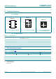
Voltages are referenced to GND (ground = 0 V); for test circuit see Figure 9.
Symbol Parameter Conditions 25 °C −40 °C to +125 °C Unit
Min Typ
[1]
Max Min Max
(85 °C)
Max
(125 °C)
Measurement points are given in Table 9.
Logic levels: V
OL
and V
OH
are typical output voltage levels that occur with the output load.
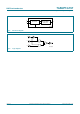
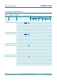
Fig 8. The data inputs (I0, I1) and common data select input (S) to output (Y) propagation delays
001aac658
I0, I1, S input
Y output
V
I
V
OH
V
OL
V
M
t
PHL
t
PLH
V
M
GND
Table 9. Measurement points
Supply voltage Output Input
V
CC
V
M
V
M
V
I
t
r
= t
f
0.8 V to 3.6 V 0.5 × V
CC
0.5 × V
CC
V
CC
≤ 3.0 ns