
Datasheet


74AUP1G157 All information provided in this document is subject to legal disclaimers. © NXP B.V. 2012. All rights reserved.
Product data sheet Rev. 5 — 22 June 2012 4 of 20
NXP Semiconductors
74AUP1G157
Low-power 2-input multiplexer
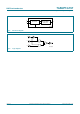
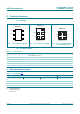
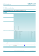
6. Pinning information
6.1 Pinning
6.2 Pin description
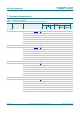
7. Functional description
[1] H = HIGH voltage level;
L = LOW voltage level;
X = don’t care.
Fig 5. Pin configuration SOT363 Fig 6. Pin configuration SOT886 Fig 7. Pin configuration SOT891,
SOT1115 and SOT1202
74AUP1G157
I1 S
GND
I0 Y
001aae015
1
2
3
6
V
CC
5
4
74AUP1G157
GND
001aae016
I1
I0
V
CC
S
Y
Transparent top view
2
3
1
5
4
6
74AUP1G157
GND
001aae017
I1
I0
V
CC
S
Y
Transparent top view
2
3
1
5
4
6
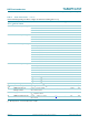
Table 3. Pin description
Symbol Pin Description
I1 1 data input from source 1
GND 2 ground (0 V)
I0 3 data input from source 0
Y 4 multiplexer output
V
CC
5 supply voltage
S 6 common data select input
Table 4. Function table
[1]
Input Output
S I1 I0 Y
LXLL
LXHH
HL XL
HHXH