
Datasheet


74AUP1G34 All information provided in this document is subject to legal disclaimers. © NXP B.V. 2012. All rights reserved.
Product data sheet Rev. 6 — 28 June 2012 2 of 20
NXP Semiconductors
74AUP1G34
Low-power buffer
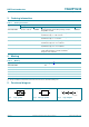
3. Ordering information
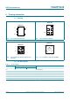
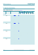
4. Marking
[1] The pin 1 indicator is located on the lower left corner of the device, below the marking code.
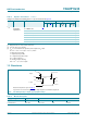
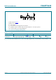
5. Functional diagram
Table 1. Ordering information
Type number Package
Temperature range Name Description Version
74AUP1G34GW −40 °C to +125 °C TSSOP5 plastic thin shrink small outline package; 5 leads;
body width 1.25 mm
SOT353-1
74AUP1G34GM −40 °C to +125 °C XSON6 plastic extremely thin small outline package; no leads;
6 terminals; body 1 × 1.45 × 0.5 mm
SOT886
74AUP1G34GF −40 °C to +125 °C XSON6 plastic extremely thin small outline package; no leads;
6 terminals; body 1 × 1 × 0.5 mm
SOT891
74AUP1G34GN −40 °C to +125 °C XSON6 extremely thin small outline package; no leads;
6 terminals; body 0.9 × 1.0 × 0.35 mm
SOT1115
74AUP1G34GS −40 °C to +125 °C XSON6 extremely thin small outline package; no leads;
6 terminals; body 1.0 × 1.0 × 0.35 mm
SOT1202
74AUP1G34GX −40 °C to +125 °C X2SON5 X2SON5: plastic thermal enhanced extremely thin
small outline package; no leads; 5 terminals;
body 0.8 × 0.8 × 0.35 mm
SOT1226
Table 2. Marking
Type number Marking code
[1]
74AUP1G34GW aN
74AUP1G34GM aN
74AUP1G34GF aN
74AUP1G34GN aN
74AUP1G34GS aN
74AUP1G34GX aN
Fig 1. Logic symbol Fig 2. IEC logic symbol Fig 3. Logic diagram
001aac538
2A 4Y
001aac537
24
001aac536
YA