
Datasheet

74AUP1G58 All information provided in this document is subject to legal disclaimers. © NXP B.V. 2012. All rights reserved.
Product data sheet Rev. 6 — 15 August 2012 9 of 22
NXP Semiconductors
74AUP1G58
Low-power configurable multiple function gate
[1] All typical values are measured at nominal V
CC
.
[2] t
pd
is the same as t
PLH
and t
PHL
.
[3] All specified values are the average typical values over all stated loads.
[4] C
PD
is used to determine the dynamic power dissipation (P
D
in W).
P
D
=C
PD
V
CC
2
f
i
N+(C
L
V
CC
2
f
o
) where:
f
i
= input frequency in MHz;
f
o
= output frequency in MHz;
C
L
= load capacitance in pF;
V
CC
= supply voltage in V;
N = number of inputs switching;
(C
L
V
CC
2
f
o
) = sum of the outputs.
C
L
= 30 pF
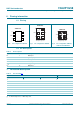
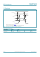
t
pd
propagation delay A, B and C to Y;
see Figure 12
[2]
V
CC
= 0.8 V - 38.0 - - - - ns
V
CC
= 1.1 V to 1.3 V 4.5 10.5 20.8 4.1 21.9 24.1 ns
V
CC
= 1.4 V to 1.6 V 3.8 7.5 12.2 3.8 13.5 14.1 ns
V
CC
= 1.65 V to 1.95 V 3.4 6.3 10.0 3.1 11.2 11.9 ns
V
CC
= 2.3 V to 2.7 V 3.4 5.3 7.5 3.1 8.4 8.9 ns
V
CC
= 3.0 V to 3.6 V 3.3 5.0 6.6 2.9 7.1 7.4 ns
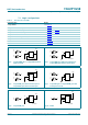
C
L
= 5 pF, 10 pF, 15 pF and 30 pF
C
PD
power dissipation
capacitance
f
i
= 1 MHz; V
I
=GNDto V
CC
[3]
[4]
V
CC
= 0.8 V - 2.7 - - - - pF
V
CC
= 1.1 V to 1.3 V - 2.8 - - - - pF
V
CC
= 1.4 V to 1.6 V - 3.0 - - - - pF
V
CC
= 1.65 V to 1.95 V - 3.2 - - - - pF
V
CC
= 2.3 V to 2.7 V - 3.8 - - - - pF
V
CC
= 3.0 V to 3.6 V - 4.4 - - - - pF
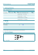
Table 9. Dynamic characteristics
…continued
Voltages are referenced to GND (ground = 0 V); for test circuit see Figure 13.
Symbol Parameter Conditions 25 C 40 C to +125 C Unit
Min Typ
[1]
Max Min Max
(85 C)
Max
(125 C)