
Datasheet

74AUP1G74 All information provided in this document is subject to legal disclaimers. © NXP B.V. 2014. All rights reserved.
Product data sheet Rev. 9 — 6 January 2014 2 of 28
NXP Semiconductors
74AUP1G74
Low-power D-type flip-flop with set and reset; positive-edge trigger
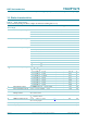
3. Ordering information
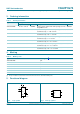
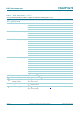
4. Marking
[1] The pin 1 indicator is located on the lower left corner of the device, below the marking code.
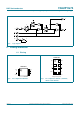
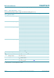
5. Functional diagram
Table 1. Ordering information
Type number Package
Temperature range Name Description Version
74AUP1G74DC 40 C to +125 C VSSOP8 plastic very thin shrink small outline package; 8 leads;
body width 2.3 mm
SOT765-1
74AUP1G74GT 40 C to +125 C XSON8 plastic extremely thin small outline package; no leads;
8 terminals; body 1 1.95 0.5 mm
SOT833-1
74AUP1G74GF 40 C to +125 C XSON8 extremely thin small outline package; no leads;
8 terminals; body 1.35 1 0.5 mm
SOT1089
74AUP1G74GD 40 Cto+125C XSON8 plastic extremely thin small outline package; no leads;
8 terminals; body 3 2 0.5 mm
SOT996-2
74AUP1G74GM 40 C to +125 C XQFN8 plastic, extremely thin quad flat package; no leads;
8 terminals; body 1.6 1.6 0.5 mm
SOT902-2
74AUP1G74GN 40 C to +125 C XSON8 extremely thin small outline package; no leads;
8 terminals; body 1.2 1.0 0.35 mm
SOT1116
74AUP1G74GS 40 C to +125 C XSON8 extremely thin small outline package; no leads;
8 terminals; body 1.35 1.0 0.35 mm
SOT1203
Table 2. Marking codes
Type number Marking code
[1]
74AUP1G74DC p74
74AUP1G74GT p74
74AUP1G74GF 54
74AUP1G74GD p74
74AUP1G74GM p74
74AUP1G74GN 54
74AUP1G74GS 54
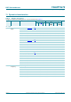
Fig 1. Logic symbol Fig 2. IEC logic symbol
001aah725
RD
FF
SD
Q
Q
Q
Q
SD
CP
CP
D
D
RD
001aah726
C1
S
1D
R