
Datasheet

74AUP1G74 All information provided in this document is subject to legal disclaimers. © NXP B.V. 2014. All rights reserved.
Product data sheet Rev. 9 — 6 January 2014 4 of 28
NXP Semiconductors
74AUP1G74
Low-power D-type flip-flop with set and reset; positive-edge trigger
6.2 Pin description
7. Functional description
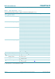
[1] H = HIGH voltage level; L = LOW voltage level; X = don’t care.
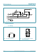
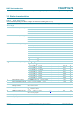
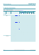
Fig 6. Pin configuration SOT996-2 Fig 7. Pin configuration SOT902-2
001aai217
74AUP1G74
Transparent top view
8
7
6
5
1
2
3
4
CP
D
Q
GND
V
CC
SD
RD
Q
001aae324
DRD
CP
V
CC
Q
SD
GND
Q
Transparent top view
3
6
4
1
5
8
7
2
terminal 1
index area
74AUP1G74
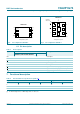
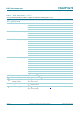
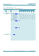
Table 3. Pin description
Symbol Pin Description
SOT765-1, SOT833-1, SOT1089,
SOT996-2, SOT1116 and SOT1203
SOT902-2
CP 1 7 clock input
D 2 6 data input
Q
3 5 complement output
GND 4 4 ground (0 V)
Q 5 3 true output
R
D 6 2 asynchronous reset input (active LOW)
S
D 7 1 asynchronous set input (active LOW)
V
CC
8 8 supply voltage
Table 4. Function table for asynchronous operation
[1]
Input Output
SD RD CP D Q Q
LHXXHL
HLXXLH
LLXXHH