
Datasheet

1. General description
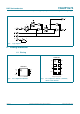
The 74AUP1G74 provides a low-power, low-voltage single positive-edge triggered D-type
flip-flop with individual data (D), clock (CP), set (S
D) and reset (RD) inputs and
complementary Q and Q
outputs. The SD and RD are asynchronous active LOW inputs
and operate independently of the clock input. Information on the data input is transferred
to the Q output on the LOW-to-HIGH transition of the clock pulse. The D input must be
stable one set-up time prior to the LOW-to-HIGH clock transition for predictable operation.
Schmitt trigger action at all inputs makes the circuit tolerant to slower input rise and fall
times across the entire V
CC
range from 0.8 V to 3.6 V.
This device ensures a very low static and dynamic power consumption across the entire
V
CC
range from 0.8 V to 3.6 V.
This device is fully specified for partial power-down applications using I
OFF
. The I
OFF
circuitry disables the output, preventing the damaging backflow current through the device
when it is powered down.
2. Features and benefits
Wide supply voltage range from 0.8 V to 3.6 V
High noise immunity
Complies with JEDEC standards:
JESD8-12 (0.8 V to 1.3 V)
JESD8-11 (0.9 V to 1.65 V)
JESD8-7 (1.2 V to 1.95 V)
JESD8-5 (1.8 V to 2.7 V)
JESD8-B (2.7 V to 3.6 V)
ESD protection:
HBM JESD22-A114F Class 3A exceeds 5000 V
MM JESD22-A115-A exceeds 200 V
CDM JESD22-C101E exceeds 1000 V
Low static power consumption; I
CC
= 0.9 A (maximum)
Latch-up performance exceeds 100 mA per JESD 78 Class II
Inputs accept voltages up to 3.6 V
Low noise overshoot and undershoot < 10 % of V
CC
I
OFF
circuitry provides partial power-down mode operation
Multiple package options
Specified from 40 Cto+85C and 40 Cto+125C
74AUP1G74
Low-power D-type flip-flop with set and reset; positive-edge
trigger
Rev. 9 — 6 January 2014 Product data sheet