
Datasheet

74AUP1G74 All information provided in this document is subject to legal disclaimers. © NXP B.V. 2014. All rights reserved.
Product data sheet Rev. 9 — 6 January 2014 5 of 28
NXP Semiconductors
74AUP1G74
Low-power D-type flip-flop with set and reset; positive-edge trigger
[1] H = HIGH voltage level;
L = LOW voltage level;
X = don’t care;
= LOW-to-HIGH CP transition;
Q
n+1
= state after the next LOW-to-HIGH CP transition.
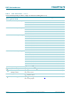
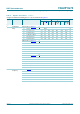
8. Limiting values
[1] The minimum input and output voltage ratings may be exceeded if the input and output current ratings are observed.
[2] For VSSOP8 packages: above 110 C the value of P
tot
derates linearly with 8.0 mW/K.
For XSON8 and XQFN8 packages: above 118 C the value of P
tot
derates linearly with 7.8 mW/K.
9. Recommended operating conditions
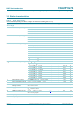
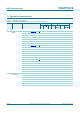
Table 5. Function table for synchronous operation
[1]
Input Output
SD RD CP D Q
n+1
Q
n+1
HH LLH
HH HHL
Table 6. Limiting values
In accordance with the Absolute Maximum Rating System (IEC 60134). Voltages are referenced to GND (ground = 0 V).
Symbol Parameter Conditions Min Max Unit
V
CC
supply voltage 0.5 +4.6 V
I
IK
input clamping current V
I
<0V 50 - mA
V
I
input voltage
[1]
0.5 +4.6 V
I
OK
output clamping current V
O
<0V 50 - mA
V
O
output voltage Active mode and Power-down mode
[1]
0.5 +4.6 V
I
O
output current V
O
=0VtoV
CC
- 20 mA
I
CC
supply current - +50 mA
I
GND
ground current 50 - mA
T
stg
storage temperature 65 +150 C
P
tot
total power dissipation T
amb
= 40 C to +125 C
[2]
-250mW
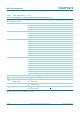
Table 7. Operating conditions
Symbol Parameter Conditions Min Max Unit
V
CC
supply voltage 0.8 3.6 V
V
I
input voltage 0 3.6 V
V
O
output voltage Active mode 0 V
CC
V
Power-down mode; V
CC
=0V 0 3.6 V
T
amb
ambient temperature 40 +125 C
t/V input transition rise and fall rate V
CC
= 0.8 V to 3.6 V - 200 ns/V