
Datasheet

1. General description
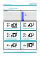
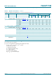
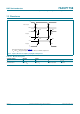
The 74AUP1T58 provides low-power, low-voltage configurable logic gate functions. The
output state is determined by eight patterns of 3-bit input. The user can choose the logic
functions AND, OR, NAND, NOR, XOR, inverter and buffer. All inputs can be connected to
V
CC
or GND.
This device ensures a very low static and dynamic power consumption across the entire
V
CC
range from 2.3 V to 3.6 V.
The 74AUP1T58 is designed for logic-level translation applications with input switching
levels that accept 1.8 V low-voltage CMOS signals, while operating from either a single
2.5 V or 3.3 V supply voltage.
The wide supply voltage range ensures normal operation as battery voltage drops from
3.6 V to 2.3 V.
This device is fully specified for partial power-down applications using I
OFF
.
The I
OFF
circuitry disables the output, preventing the damaging backflow current through
the device when it is powered down.
Schmitt trigger inputs make the circuit tolerant to slower input rise and fall times across
the entire V
CC
range.
2. Features and benefits
Wide supply voltage range from 2.3 V to 3.6 V
High noise immunity
ESD protection:
HBM JESD22-A114F Class 3A exceeds 5000 V
MM JESD22-A115-A exceeds 200 V
CDM JESD22-C101E exceeds 1000 V
Low static power consumption; I
CC
= 1.5 A (maximum)
Latch-up performance exceeds 100 mA per JESD 78B Class II
Inputs accept voltages up to 3.6 V
Low noise overshoot and undershoot < 10 % of V
CC
I
OFF
circuitry provides partial power-down mode operation
Multiple package options
Specified from 40 Cto+85C and 40 Cto+125C
74AUP1T58
Low-power configurable gate with voltage-level translator
Rev. 5 — 15 August 2012 Product data sheet