
Datasheet


74AUP2G0604 All information provided in this document is subject to legal disclaimers. © NXP B.V. 2012. All rights reserved.
Product data sheet Rev. 1 — 23 November 2012 10 of 20
NXP Semiconductors
74AUP2G0604
Low-power inverting buffer with open-drain and inverter
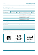
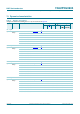
12. Waveforms
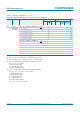
Measurement points are given in Table 10.
Logic levels: V
OL
and V
OH
are typical output voltage levels that occur with the output load.
Fig 7. The data input 1A to output 1Y and input 2A to output 2Y propagation delays
W
3+/
W
3/+
9
0
9
0
9
0
9
0
*1'
9
,
9
2+
9
2/
$LQSXW
<RXWSXW
W
3/=
9
;
$LQSXW
<RXWSXW
9
,
9
&&
9
0
9
2/
*1'
W
3=/
9
0
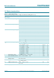
Table 10. Measurement points
Supply voltage Output Input
V
CC
V
M
V
X
V
M
V
I
t
r
= t
f
0.8 V to 1.6 V 0.5 V
CC
V
OL
+ 0.1 V 0.5 V
CC
V
CC
3.0 ns
1.65 V to 2.7 V 0.5 V
CC
V
OL
+ 0.15 V 0.5 V
CC
V
CC
3.0 ns
3.0 V to 3.6 V 0.5 V
CC
V
OL
+ 0.3 V 0.5 V
CC
V
CC
3.0 ns