
Datasheet


74AUP2G0604 All information provided in this document is subject to legal disclaimers. © NXP B.V. 2012. All rights reserved.
Product data sheet Rev. 1 — 23 November 2012 3 of 20
NXP Semiconductors
74AUP2G0604
Low-power inverting buffer with open-drain and inverter
6. Pinning information
6.1 Pinning
6.2 Pin description
7. Functional description
[1] H = HIGH voltage level; L = LOW voltage level.
[1] H = HIGH voltage level; L = LOW voltage level.
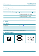
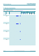
Fig 4. Pin configuration SOT363 Fig 5. Pin configuration SOT886 Fig 6. Pin configuration SOT891,
SOT1115 and SOT1202
DDD
<
<
9
&&
$
*1'
$
$83*
DDD
9
&&
<
<
*1'
$
$
7UDQVSDUHQWWRSYLHZ
$83*
DDD
*1'
$
$
9
&&
<
<
7UDQVSDUHQWWRSYLHZ
$83*
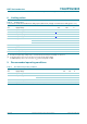
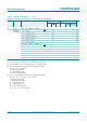
Table 3. Pin description
Symbol Pin Description
1A 1 data input
GND 2 ground (0 V)
2A 3 data input
2Y 4 data output
V
CC
5 supply voltage
1Y 6 data output
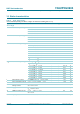
Table 4. Function table
[1]
Input Output
1A 1Y
LZ
HL
Table 5. Function table
[1]
Input Output
2A 2Y
LH
HL