
Datasheet

1. General description
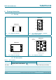
The 74AUP2G126 provides the dual non-inverting buffer/line driver with 3-state output.
The 3-state output is controlled by the output enable input (nOE). A LOW level at pin nOE
causes the output to assume a high-impedance OFF-state. This device has the
input-disable feature, which allows floating input signals. The inputs are disabled when the
output enable input nOE is LOW.
Schmitt trigger action at all inputs makes the circuit tolerant to slower input rise and fall
times across the entire V
CC
range from 0.8 V to 3.6 V. This device ensures a very low
static and dynamic power consumption across the entire V
CC
range from 0.8 V to 3.6 V.
This device is fully specified for partial power-down applications using I
OFF
. The I
OFF
circuitry disables the output, preventing a damaging backflow current through the device
when it is powered down.
2. Features and benefits
Wide supply voltage range from 0.8 V to 3.6 V
High noise immunity
Complies with JEDEC standards:
JESD8-12 (0.8 V to 1.3 V)
JESD8-11 (0.9 V to 1.65 V)
JESD8-7 (1.2 V to 1.95 V)
JESD8-5 (1.8 V to 2.7 V)
JESD8-B (2.7 V to 3.6 V)
ESD protection:
HBM JESD22-A114F Class 3A exceeds 5000 V
MM JESD22-A115-A exceeds 200 V
CDM JESD22-C101E exceeds 1000 V
Low static power consumption; I
CC
= 0.9 A (maximum)
Latch-up performance exceeds 100 mA per JESD78 Class II
Inputs accept voltages up to 3.6 V
Low noise overshoot and undershoot < 10 % of V
CC
Input-disable feature allows floating input conditions
I
OFF
circuitry provides partial Power-down mode operation
Multiple package options
Specified from 40 Cto+85C and 40 Cto+125C
74AUP2G126
Low-power dual buffer/line driver; 3-state
Rev. 9 — 11 February 2013 Product data sheet