
Datasheet

74AUP2G126 All information provided in this document is subject to legal disclaimers. © NXP B.V. 2013. All rights reserved.
Product data sheet Rev. 9 — 11 February 2013 3 of 24
NXP Semiconductors
74AUP2G126
Low-power dual buffer/line driver; 3-state
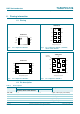
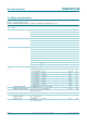
6. Pinning information
6.1 Pinning
6.2 Pin description
Fig 3. Pin configuration SOT765-1 Fig 4. Pin configuration SOT833-1, SOT1089,
SOT1116 and SOT1203
74AUP2G126
1OE V
CC
1A 2OE
2Y 1Y
GND 2A
001aae997
1
2
3
4
6
5
8
7
74AUP2G126
1Y
2OE
V
CC
2A
2Y
1A
1OE
GND
001aae998
36
27
18
45
Transparent top view
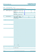
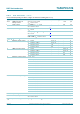
Fig 5. Pin configuration SOT996-2 Fig 6. Pin configuration SOT902-2
001aaj474
74AUP2G126
Transparent top view
8
7
6
5
1
2
3
4
1OE
1A
2Y
GND
V
CC
2OE
1Y
2A
001aae999
1A1Y
1OE
V
CC
2Y
2OE
GND
2A
Transparent top view
3
6
4
1
5
8
7
2
terminal 1
index area
74AUP2G126
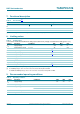
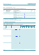
Table 3. Pin description
Symbol Pin Description
SOT765-1, SOT833-1, SOT1089,
SOT996-2, SOT1116 and SOT1203
SOT902-2
1OE, 2OE 1, 7 7, 1 output enable input (active HIGH)
1A, 2A 2, 5 6, 3 data input
1Y, 2Y 6, 3 2, 5 data output
GND 4 4 ground (0 V)
V
CC
8 8 supply voltage