
Datasheet


74AUP2G132 All information provided in this document is subject to legal disclaimers. © NXP B.V. 2013. All rights reserved.
Product data sheet Rev. 7 — 8 February 2013 10 of 23
NXP Semiconductors
74AUP2G132
Low-power dual 2-input NAND Schmitt trigger
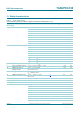
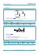
14. Transfer characteristics
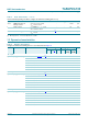
15. Waveforms transfer characteristics
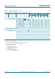
Table 11. Transfer characteristics
Voltages are referenced to GND (ground = 0 V; for test circuit see Figure 9.
Symbol Parameter Conditions T
amb
= 25 C T
amb
= 40 C to +125 C Unit
Min Typ Max Min Max
(85 C)
Max
(125 C)
V
T+
positive-going
threshold voltage
see Figure 10 and
Figure 11
V
CC
= 0.8 V 0.30 - 0.60 0.30 0.60 0.62 V
V
CC
= 1.1 V 0.53 - 0.90 0.53 0.90 0.92 V
V
CC
= 1.4 V 0.74 - 1.11 0.74 1.11 1.13 V
V
CC
= 1.65 V 0.91 - 1.29 0.91 1.29 1.31 V
V
CC
= 2.3 V 1.37 - 1.77 1.37 1.77 1.80 V
V
CC
= 3.0 V 1.88 - 2.29 1.88 2.29 2.32 V
V
T
negative-going
threshold voltage
see Figure 10 and
Figure 11
V
CC
= 0.8 V 0.10 - 0.60 0.10 0.60 0.60 V
V
CC
= 1.1 V 0.26 - 0.65 0.26 0.65 0.65 V
V
CC
= 1.4 V 0.39 - 0.75 0.39 0.75 0.75 V
V
CC
= 1.65 V 0.47 - 0.84 0.47 0.84 0.84 V
V
CC
= 2.3 V 0.69 - 1.04 0.69 1.04 1.04 V
V
CC
= 3.0 V 0.88 - 1.24 0.88 1.24 1.24 V
V
H
hysteresis voltage (V
T+
V
T
); see Figure 10,
Figure 11, Figure 12 and
Figure 13
V
CC
= 0.8 V 0.07 - 0.50 0.07 0.50 0.50 V
V
CC
= 1.1 V 0.08 - 0.46 0.08 0.46 0.46 V
V
CC
= 1.4 V 0.18 - 0.56 0.18 0.56 0.56 V
V
CC
= 1.65 V 0.27 - 0.66 0.27 0.66 0.66 V
V
CC
= 2.3 V 0.53 - 0.92 0.53 0.92 0.92 V
V
CC
= 3.0 V 0.79 - 1.31 0.79 1.31 1.31 V
V
T+
and V
T
limits at 70 % and 20 %.
Fig 10. Transfer characteristic Fig 11. Definition of V
T+
, V
T
and V
H
mna207
V
O
V
I
V
H
V
T+
V
T−
mna208
V
O
V
I
V
H
V
T+
V
T−