
Datasheet


74AUP2G132 All information provided in this document is subject to legal disclaimers. © NXP B.V. 2013. All rights reserved.
Product data sheet Rev. 7 — 8 February 2013 9 of 23
NXP Semiconductors
74AUP2G132
Low-power dual 2-input NAND Schmitt trigger
13. Waveforms
[1] R
L
= 5 k when measuring enable and disable times. R
L
= 1 M when measuring propagation delays, setup and hold times and pulse
width.
Measurement points are given in Table 9
.
Logic levels: V
OL
and V
OH
are typical output voltage levels that occur with the output load.
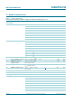
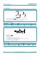
Fig 8. The data input (nA or nB) to output (nY) propagation delays
001aaj265
nA, nB input
V
T−
nY output
V
M
V
M
t
PHL
t
PLH
V
OH
V
OL
V
T+
Table 9. Measurement points
Supply voltage Output Input
V
CC
V
M
V
M
V
I
t
r
= t
f
0.8 V to 3.6 V 0.5 V
CC
0.5 V
CC
V
CC
3.0 ns
Test data is given in Table 10.
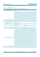
Definitions for test circuit:
R
L
= Load resistance.
C
L
= Load capacitance including jig and probe capacitance.
R
T
= Termination resistance should be equal to the output impedance Z
o
of the pulse generator.
V
EXT
= External voltage for measuring switching times.
Fig 9. Test circuit for measuring switching times
001aac521
DUT
R
T
V
I
V
O
V
EXT
V
CC
R
L
5 kΩ
C
L
G
Table 10. Test data
Supply voltage Load V
EXT
V
CC
C
L
R
L
[1]
t
PLH
, t
PHL
t
PZH
, t
PHZ
t
PZL
, t
PLZ
0.8 V to 3.6 V 5 pF, 10 pF, 15 pF and 30 pF 5 k or 1 M open GND 2 V
CC