
Datasheet


74AUP2G14 All information provided in this document is subject to legal disclaimers. © NXP B.V. 2012. All rights reserved.
Product data sheet Rev. 5 — 4 December 2012 11 of 21
NXP Semiconductors
74AUP2G14
Low-power dual Schmitt trigger inverter
16. Application information
The slow input rise and fall times cause additional power dissipation, this can be
calculated using the following formula:
P
add
=f
i
(t
r
I
CC(AV)
+t
f
I
CC(AV)
) V
CC
where:
P
add
= additional power dissipation (W);
f
i
= input frequency (MHz);
t
r
=rise time (ns); 10%to90%;
t
f
= fall time (ns); 90 % to 10 %;
I
CC(AV)
= average additional supply current (A).
Average I
CC(AV)
differs with positive or negative input transitions, as shown in Figure 13.
An example of a relaxation circuit using the 74AUP2G14 is shown in Figure 14
.
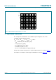
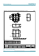
Fig 12. Typical transfer characteristics; V
CC
= 3.0 V
001aad692
V
I
(V)
0 3.02.01.0
400
800
1200
I
CC
(μA)
0