
Datasheet


74AUP2G17 All information provided in this document is subject to legal disclaimers. © NXP B.V. 2012. All rights reserved.
Product data sheet Rev. 6 — 4 December 2012 10 of 21
NXP Semiconductors
74AUP2G17
Low-power dual Schmitt trigger
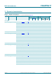
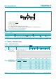
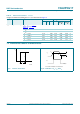
14. Waveforms transfer characteristics
V
H
hysteresis voltage (V
T+
V
T
); see Figure 9,
Figure 10, Figure 11 and
Figure 12
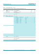
V
CC
= 0.8 V 0.07 - 0.50 0.07 0.50 0.50 V
V
CC
= 1.1 V 0.08 - 0.46 0.08 0.46 0.46 V
V
CC
= 1.4 V 0.18 - 0.56 0.18 0.56 0.56 V
V
CC
= 1.65 V 0.27 - 0.66 0.27 0.66 0.66 V
V
CC
= 2.3 V 0.53 - 0.92 0.53 0.92 0.92 V
V
CC
= 3.0 V 0.79 - 1.31 0.79 1.31 1.31 V
Table 11. Transfer characteristics
…continued
Voltages are referenced to GND (ground = 0 V; for test circuit see Figure 8.
Symbol Parameter Conditions 25 C 40 C to +125 C Unit
Min Typ Max Min Max
(85 C)
Max
(125 C)
V
T+
and V
T
limits at 70 % and 20 %.
Fig 9. Transfer characteristic Fig 10. Definition of V
T+
, V
T
and V
H
mnb154
V
O
V
H
V
I
V
T+
V
T−
mnb155
V
O
V
I
V
H
V
T+
V
T−