
Datasheet


74AUP2G241 All information provided in this document is subject to legal disclaimers. © NXP B.V. 2013. All rights reserved.
Product data sheet Rev. 7 — 11 February 2013 14 of 26
NXP Semiconductors
74AUP2G241
Low-power dual buffer/line driver; 3-state
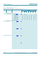
Measurement points are given in Table 10.
Logic levels: V
OL
and V
OH
are typical output voltage levels that occur with the output load.
Fig 8. 3-state enable and disable times
001aaa411
t
PLZ
t
PHZ
outputs
disabled
outputs
enabled
outputs
enabled
output
LOW-to-OFF
OFF-to-LOW
output
HIGH-to-OFF
OFF-to-HIGH
1OE input
V
I
V
OL
V
OH
V
CC
V
M
GND
GND
t
PZL
t
PZH
V
M
V
M
V
OH
− 0.3 V
V
OL
+ 0.3 V
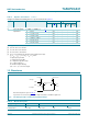
Measurement points are given in Table 10.
Logic levels: V
OL
and V
OH
are typical output voltage levels that occur with the output load.
Fig 9. 3-state enable and disable times
001aaa410
t
PLZ
t
PHZ
outputs
disabled
outputs
enabled
V
OH
− 0.3 V
V
OL
+ 0.3 V
outputs
enabled
output
LOW-to-OFF
OFF-to-LOW
output
HIGH-to-OFF
OFF-to-HIGH
2OE input
V
I
V
OL
V
OH
V
CC
V
M
GND
GND
t
PZL
t
PZH
V
M
V
M
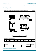
Table 10. Measurement points
Supply voltage Input Output
V
CC
V
M
V
M
V
X
V
Y
0.8 V to 1.6 V 0.5 V
CC
0.5 V
CC
V
OL
0.1 V V
OH
0.1 V
1.65 V to 2.7 V 0.5 V
CC
0.5 V
CC
V
OL
0.15 V V
OH
0.15 V
3.0 V to 3.6 V 0.5 V
CC
0.5 V
CC
V
OL
0.3 V V
OH
0.3 V