
Datasheet

74AUP2G86 All information provided in this document is subject to legal disclaimers. © NXP B.V. 2013. All rights reserved.
Product data sheet Rev. 8 — 24 January 2013 4 of 21
NXP Semiconductors
74AUP2G86
Low-power dual 2-input EXCLUSIVE-OR gate
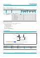
6.2 Pin description
7. Functional description
[1] H = HIGH voltage level;
L = LOW voltage level.
8. Limiting values
[1] The input and output voltage ratings may be exceeded if the input and output current ratings are observed.
[2] For VSSOP8 packages: above 110 C the value of P
tot
derates linearly with 8.0 mW/K.
For XSON8 and XQFN8 packages: above 118 C the value of P
tot
derates linearly with 7.8 mW/K.
Table 3. Pin description
Symbol Pin Description
SOT765-1, SOT833-1, SOT1089,
SOT996-2, SOT1116 and SOT1203
SOT902-2
1A, 2A 1, 5 7, 3 data input
1B, 2B 2, 6 6, 2 data input
GND 4 4 ground (0 V)
1Y, 2Y 7, 3 1, 5 data output
V
CC
8 8 supply voltage
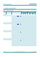
Table 4. Function table
[1]
Input Output
nA nB nY
LL L
LH H
HL H
HH L
Table 5. Limiting values
In accordance with the Absolute Maximum Rating System (IEC 60134). Voltages are referenced to GND (ground = 0 V).
Symbol Parameter Conditions Min Max Unit
V
CC
supply voltage 0.5 +4.6 V
I
IK
input clamping current V
I
<0V 50 - mA
V
I
input voltage
[1]
0.5 +4.6 V
I
OK
output clamping current V
O
<0V 50 - mA
V
O
output voltage Active mode and Power-down mode
[1]
0.5 +4.6 V
I
O
output current V
O
=0 VtoV
CC
- 20 mA
I
CC
supply current - 50 mA
I
GND
ground current 50 - mA
T
stg
storage temperature 65 +150 C
P
tot
total power dissipation T
amb
= 40 C to +125 C
[2]
- 250 mW