
Datasheet

74AVC4TD245 All information provided in this document is subject to legal disclaimers. © NXP B.V. 2011. All rights reserved.
Product data sheet Rev. 2 — 9 December 2011 11 of 26
NXP Semiconductors
74AVC4TD245
4-bit dual supply translating transceiver; 3-state
[1] t
pd
is the same as t
PLH
and t
PHL
; t
dis
is the same as t
PLZ
and t
PHZ
; t
en
is the same as t
PZL
and t
PZH
.
[1] t
pd
is the same as t
PLH
and t
PHL
; t
dis
is the same as t
PLZ
and t
PHZ
; t
en
is the same as t
PZL
and t
PZH
.
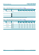
Table 11. Typical dynamic characteristics at V
CC(A)
= 0.8 V and T
amb
= 25 C
[1]
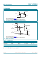
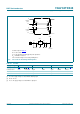
Voltages are referenced to GND (ground = 0 V); for test circuit see Figure 8; for wave forms see Figure 6 and Figure 7
Symbol Parameter Conditions V
CC(B)
Unit
0.8 V 1.2 V 1.5 V 1.8 V 2.5 V 3.3 V
t
pd
propagation delay An to Bn 14.5 7.3 6.5 6.2 5.9 6.0 ns
Bn to An 14.5 12.7 12.4 12.3 12.1 12.0 ns
t
dis
disable time OE to An 14.3 14.3 14.3 14.3 14.3 14.3 ns
OE
to Bn 17.0 9.9 9.0 9.4 9.0 9.7 ns
t
en
enable time OE to An 18.2 18.2 18.2 18.2 18.2 18.2 ns
OE
to Bn 19.2 10.7 9.8 9.6 9.7 10.2 ns
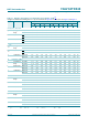
Table 12. Typical dynamic characteristics at V
CC(B)
= 0.8 V and T
amb
= 25 C
[1]
Voltages are referenced to GND (ground = 0 V); for test circuit see Figure 8; for wave forms see Figure 6 and Figure 7
Symbol Parameter Conditions V
CC(A)
Unit
0.8 V 1.2 V 1.5 V 1.8 V 2.5 V 3.3 V
t
pd
propagation delay An to Bn 14.5 12.7 12.4 12.3 12.1 12.0 ns
Bn to An 14.5 7.3 6.5 6.2 5.9 6.0 ns
t
dis
disable time OE to An 14.3 5.5 4.1 4.0 3.0 3.5 ns
OE
to Bn 17.0 13.8 13.4 13.1 12.9 12.7 ns
t
en
enable time OE to An 18.2 5.6 4.0 3.2 2.4 2.2 ns
OE
to Bn 19.2 14.6 14.1 13.9 13.7 13.6 ns