
Datasheet


74AVC4TD245 All information provided in this document is subject to legal disclaimers. © NXP B.V. 2011. All rights reserved.
Product data sheet Rev. 2 — 9 December 2011 3 of 26
NXP Semiconductors
74AVC4TD245
4-bit dual supply translating transceiver; 3-state
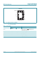
6. Pinning information
6.1 Pinning
Fig 2. Logic diagram (one 1-bit transceiver)
001aao070
V
CC(A)
V
CC(B)
Bn
to next transceiver
OE
An
DIRn
(1) This is not a supply pin, the substrate is attached to this
pad using conductive die attach material. There is no
electrical or mechanical requirement to solder this pad
however if it is soldered the solder land should remain
floating or be connected to GND.
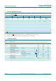
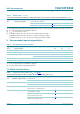
Fig 3. Pin configuration SOT403-1 (TSSOP16) Fig 4. Pin configuration SOT763-1 (DHVQFN16)
74AVC4TD245
V
CC(A)
V
CC(B)
DIR1 DIR2
A1 B1
A2 B2
A3 B3
A4 B4
DIR4 DIR3
GND OE
001aao072
1
2
3
4
5
6
7
8
10
9
12
11
14
13
16
15
001aao071
GND
(1)
74AVC4TD245
DIR4 DIR3
A4 B4
A3 B3
A2 B2
A1 B1
DIR1 DIR2
GND
OE
V
CC(A)
V
CC(B)
Transparent top view
7 10
6 11
5 12
4
13
3 14
2 15
8
9
1
16
terminal 1
index area