
Datasheet


74AVCH16T245 All information provided in this document is subject to legal disclaimers. © NXP B.V. 2012. All rights reserved.
Product data sheet Rev. 5 — 1 March 2012 6 of 29
NXP Semiconductors
74AVCH16T245
16-bit dual supply translating transceiver; 3-state
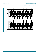
5.2 Pin description
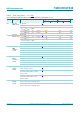
[1] All GND pins must be connected to ground (0 V).
6. Functional description
[1] H = HIGH voltage level; L = LOW voltage level; X = don’t care; Z = high-impedance OFF-state.
[2] The nAn, nDIR and nOE
input circuit is referenced to V
CC(A)
; The nBn input circuit is referenced to V
CC(B)
.
[3] If at least one of V
CC(A)
or V
CC(B)
is at GND level, the device goes into suspend mode.
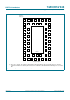
Table 2. Pin description
Symbol Pin Description
SOT362-1 and
SOT480-1
SOT702-1 SOT1134-2
1DIR, 2DIR 1, 24 A1, K1 A30, A13 direction control
1B1 to 1B8 2, 3, 5, 6, 8, 9, 11, 12 B2, B1, C2, C1,
D2, D1, E2, E1
B20, A31, D5, D1,
A2, B2, B3, A5
data input or output
2B1 to 2B8 13, 14, 16, 17, 19, 20,
22, 23
F1, F2, G1, G2,
H1, H2, J1, J2
A6, B5, B6, A9, D2,
D6, A12, B8
data input or output
GND
[1]
4, 10, 15, 21, 28, 34,
39, 45
B3, D3, G3, J3, J4,
G4, D4, B4
A32, A3, A8, A11,
A16, A19, A24, A27
ground (0 V)
V
CC(B)
7, 18 C3, H3 A1, A10 supply voltage B (nBn inputs are
referenced to V
CC(B)
)
1OE
, 2OE 48, 25 A6, K6 A29, A14 output enable input (active LOW)
1A1 to 1A8 47, 46, 44, 43, 41, 40,
38, 37
B5, B6, C5, C6,
D5, D6, E5, E6
B18, A28, D8, D4,
A25, B16, B15, A22
data input or output
2A1 to 2A8 36, 35, 33, 32, 30, 29,
27, 26
F6, F5, G6, G5,
H6, H5, J6, J5
A21, B13, B12, A18,
D3, D7, A15, B10
data input or output
V
CC(A)
31, 42 C4, H4 A17, A26 supply voltage A (nAn, nOE and nDIR
inputs are referenced to V
CC(A)
)
n.c. - A2, A3, A4, A5, K2,
K3, K4, K5
A4, A7, A20, A23,
B1, B4, B7, B9, B11,
B14, B17, B19
not connected
Table 3. Function table
[1]
Supply voltage Input Input/output
[3]
V
CC(A)
, V
CC(B)
nOE
[2]
nDIR
[2]
nAn
[2]
nBn
[2]
0.8 V to 3.6 V L L nAn = nBn input
0.8 V to 3.6 V L H input nBn = nAn
0.8 V to 3.6 V H X Z Z
GND
[3]
XXZZ