
Datasheet

1. General description
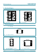
The 74AVCH2T45 is a dual bit, dual supply transceiver that enables bidirectional level
translation. It features two data input-output ports (nA and nB), a direction control input
(DIR) and dual supply pins (V
CC(A)
and V
CC(B)
). Both V
CC(A)
and V
CC(B)
can be supplied at
any voltage between 0.8 V and 3.6 V making the device suitable for translating between
any of the low voltage nodes (0.8 V, 1.2 V, 1.5 V, 1.8 V, 2.5 V and 3.3 V). Pins nA and DIR
are referenced to V
CC(A)
and pins nB are referenced to V
CC(B)
. A HIGH on DIR allows
transmission from nA to nB and a LOW on DIR allows transmission from nB to nA.
The device is fully specified for partial power-down applications using I
OFF
. The I
OFF
circuitry disables the output, preventing any damaging backflow current through the
device when it is powered down. In suspend mode when either V
CC(A)
or V
CC(B)
are at
GND level, both A and B are in the high-impedance OFF-state.
The 74AVCH2T45 has active bus hold circuitry which is provided to hold unused or
floating data inputs at a valid logic level. This feature eliminates the need for external
pull-up or pull-down resistors.
2. Features and benefits
Wide supply voltage range:
V
CC(A)
: 0.8 V to 3.6 V
V
CC(B)
: 0.8 V to 3.6 V
High noise immunity
Complies with JEDEC standards:
JESD8-12 (0.8 V to 1.3 V)
JESD8-11 (0.9 V to 1.65 V)
JESD8-7 (1.2 V to 1.95 V)
JESD8-5 (1.8 V to 2.7 V)
JESD8-B (2.7 V to 3.6 V)
ESD protection:
HBM JESD22-A114F Class 3B exceeds 8000 V
MM JESD22-A115-A exceeds 200 V
CDM JESD22-C101C exceeds 1000 V
Maximum data rates:
500 Mbps (1.8 V to 3.3 V translation)
320 Mbps (< 1.8 V to 3.3 V translation)
320 Mbps (translate to 2.5 V or 1.8 V)
74AVCH2T45
Dual-bit, dual-supply voltage level translator/transceiver;
3-state
Rev. 6 — 2 April 2013 Product data sheet