
Datasheet

74AVCH2T45 All information provided in this document is subject to legal disclaimers. © NXP B.V. 2013. All rights reserved.
Product data sheet Rev. 6 — 2 April 2013 10 of 27
NXP Semiconductors
74AVCH2T45
Dual-bit, dual-supply voltage level translator/transceiver; 3-state
11. Dynamic characteristics
[1] t
pd
is the same as t
PLH
and t
PHL
; t
dis
is the same as t
PLZ
and t
PHZ
; t
en
is the same as t
PZL
and t
PZH
.
t
en
is a calculated value using the formula shown in Section 13.4 “Enable times”
[1] t
pd
is the same as t
PLH
and t
PHL
; t
dis
is the same as t
PLZ
and t
PHZ
; t
en
is the same as t
PZL
and t
PZH
.
t
en
is a calculated value using the formula shown in Section 13.4 “Enable times”
[1] C
PD
is used to determine the dynamic power dissipation (P
D
in W).
P
D
=C
PD
V
CC
2
f
i
N+(C
L
V
CC
2
f
o
) where:
f
i
= input frequency in MHz;
f
o
= output frequency in MHz;
C
L
= load capacitance in pF;
V
CC
= supply voltage in V;
N = number of inputs switching;
(C
L
V
CC
2
f
o
) = sum of the outputs.
[2] f
i
= 10 MHz; V
I
=GNDtoV
CC
; t
r
= t
f
= 1 ns; C
L
= 0 pF; R
L
= .
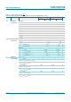
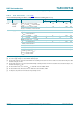
Table 9. Typical dynamic characteristics at V
CC(A)
= 0.8 V and T
amb
= 25 C
[1]
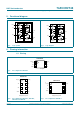
Voltages are referenced to GND (ground = 0 V); for test circuit see Figure 8; for wave forms see Figure 6 and Figure 7
Symbol Parameter Conditions V
CC(B)
Unit
0.8 V 1.2 V 1.5 V 1.8 V 2.5 V 3.3 V
t
pd
propagation delay A to B 15.8 8.4 8.0 8.0 8.7 9.5 ns
B to A 15.8 12.7 12.4 12.2 12.0 11.8 ns
t
dis
disable time DIR to A 12.2 12.2 12.2 12.2 12.2 12.2 ns
DIR to B 11.7 7.9 7.6 8.2 8.7 10.2 ns
t
en
enable time DIR to A 27.5 20.6 20.0 20.4 20.7 22.0 ns
DIR to B 28.0 20.6 20.2 20.2 20.9 21.7 ns
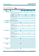
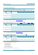
Table 10. Typical dynamic characteristics at V
CC(B)
= 0.8 V and T
amb
= 25 C
[1]
Voltages are referenced to GND (ground = 0 V); for test circuit see Figure 8; for wave forms see Figure 6 and Figure 7
Symbol Parameter Conditions V
CC(A)
Unit
0.8 V 1.2 V 1.5 V 1.8 V 2.5 V 3.3 V
t
pd
propagation delay A to B 15.8 12.7 12.4 12.2 12.0 11.8 ns
B to A 15.8 8.4 8.0 8.0 8.7 9.5 ns
t
dis
disable time DIR to A 12.2 4.9 3.8 3.7 2.8 3.4 ns
DIR to B 11.7 9.2 9.0 8.8 8.7 8.6 ns
t
en
enable time DIR to A 27.5 17.6 17.0 16.8 17.4 18.1 ns
DIR to B 28.0 17.6 16.2 15.9 14.8 15.2 ns
Table 11. Typical power dissipation capacitance at V
CC(A)
= V
CC(B)
and T
amb
= 25 C
[1][2]
Voltages are referenced to GND (ground = 0 V).
Symbol Parameter Conditions V
CC(A)
and V
CC(B)
Unit
0.8 V 1.2 V 1.5 V 1.8 V 2.5 V 3.3 V
C
PD
power dissipation
capacitance
A port: (direction A to B);
B port: (direction B to A)
122222pF
A port: (direction B to A);
B port: (direction A to B)
91111121417pF