
Datasheet

74AVCH2T45 All information provided in this document is subject to legal disclaimers. © NXP B.V. 2013. All rights reserved.
Product data sheet Rev. 6 — 2 April 2013 4 of 27
NXP Semiconductors
74AVCH2T45
Dual-bit, dual-supply voltage level translator/transceiver; 3-state
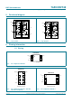
6.2 Pin description
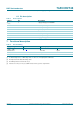
7. Functional description
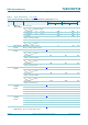
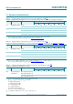
[1] H = HIGH voltage level; L = LOW voltage level; X = don’t care; Z = high-impedance OFF-state.
[2] The input circuit of the data I/O is always active.
[3] The DIR input circuit is referenced to V
CC(A)
.
[4] If at least one of V
CC(A)
or V
CC(B)
is at GND level, the device goes into suspend mode.
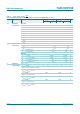
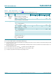
Table 3. Pin description
Symbol Pin Description
V
CC(A)
1 supply voltage port A and DIR
1A 2 data input or output
2A 3 data input or output
GND 4 ground (0 V)
DIR 5 direction control
2B 6 data input or output
1B 7 data input or output
V
CC(B)
8 supply voltage port B
Table 4. Function table
[1]
Supply voltage Input Input/output
[2]
V
CC(A)
, V
CC(B)
DIR
[3]
nA nB
0.8 V to 3.6 V L nA = nB input
0.8 V to 3.6 V H input nB = nA
GND
[4]
XZZ